
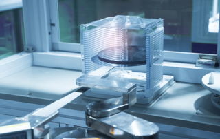
WAFER QA/QC AFTER SLICING AND POLISHING
Industry Semiconductor Applications Wafer Qa/Qc After Slicing And Polishing Measurement Type Surface Description When wafers are sliced up with wire saws, they are measured to make sure they are within the specified thickness, with minimal bow, warp, and TTV. After initial measurement, they are sorted and sent for polishing. Since polishing removes material and smoothes out the rough surfaces they need to be measured again to ensure they meet thickness guidelines and quality standards. Solution: MTI Instruments manufactures multiple systems to perform thickness measurements. From semi automated Proforma 300SA to manual wafer [...]
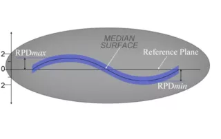
ABOUT WAFER BOW AND WARP MEASUREMENT SYSTEMS
Thickness Measurement for Metrology Systems ASTM F657: The distance through a wafer between corresponding points on the front and back surface. Thickness is expressed in microns or mils (thousandths of an inch). Total Thickness Variation (TTV) ASTM F657: The difference between the maximum and minimum values of thickness encountered during a scan pattern or series of point measurements. TTV is expressed in microns or mils (thousandths of an inch). ASTM F534 3.1.2: The deviation of the center point of the median surface of a free, unclamped wafer from the median [...]

LITHOGRAPHY OPTICS POSITION FOCUS
Industry Semiconductor Applications Photolithography Using Capacitance Sensors Measurement Type Positioning Description One specific area where capacitance systems excel is high resolution focusing of complex lens systems such as those found in atomic force microscopes, vision inspection machines and photolithography tools. In a multi-million dollar photolithography tool, high accuracy, nanometer resolution and maximum thermal stability are absolutely critical to maintain proper focus and obtain integrated circuit line widths as small as 45 nanometers. Additionally, most systems demand low power consumption and maximum heat dissipation to eliminate any adverse affects from [...]
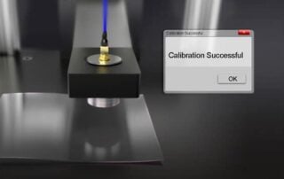
GAAS SUBSTRATE THICKNESS MEASUREMENT
Industry Semiconductor Applications Gaas Substrate Thickness Measurement Measurement Type Thickness Description Measuring Thickness of Wafers with Different Chemistries Introduction: Silicon wafers are ordinarily highly conductive and easy to measure with standard capacitive displacement sensors (See MTI’s Proforma 300i). Measuring the thickness of GaAs wafers that have high bulk resistivity (>10k Ohm/cm) is a little more difficult because the wafers act as non-conductive insulators in a capacitive sensor’s measuring field. Fortunately, MTI has a solution to this problem. Solution: It’s possible to measure the thickness and TTV of high resistivity semiconducting wafers (like GaAs) using non-contact capacitive [...]



Spindle Run Out
Industry Automotive Applications Spindle Run Out Measurement Type Positioning Description Rotating targets frequently have an intermittent, uncertain or nonexistent ground path. This introduces unwanted noise, instability, drift and reduces accuracy of the measurement. MTI Instruments offers a unique “Push-Pull” capacitance measurement system that does not require a grounded target. It utilizes two probes, built into one body, that work together to complete the ground path. One probe pushes current into the brake rotor while the adjacent probe pulls the current out. The result is a “clean”, consistent electrical sensing path. As the [...]
CAPACITANCE SENSORS FACILITATE 3D IC CONSTRUCTION
[Application Note 70518] To boost device performance, today’s semiconductor and microelectronics manufacturers are building three-dimensional integrated circuits featuring vertically-stacked silicon wafers and dies. The rationale is simple. Exploiting the Z-axis avoids the power and footprint penalties associated with two-dimensional processes. Implementing the rationale, however, is not so simple. Going vertical requires coplanar surfaces to make contact with all pins, pads, and pillars. Problem Typically, manufacturers measure the angle and gap between two planes to determine coplanarity. Bonding tool actuators rely on these angle/gap measurements to adjust components and make sure all device pins and/or solder balls reside on the [...]
CAMERA SHIELD MEASUREMENT
Equipment Setup Equipment Used DTS-25-04 laser head Rotary Stage PC with Digital Microtrak Basic Support software Setup Power is automatic mode. Filter is 100Hz Sample rate is 1000 samples sec The head was operated in diffuse mode (not specular/tilted) Validation of Setup The setup should be validated by performing a total runout scan on the rotary stage with no target present. The stage should be cleaned with Isopropyl alcohol and allowed to dry prior to the scan. This reduces any dust or dirt accumulation which will give a false reading of runout. A 360-degree runout of the rotary table, [...]
MONITOR ROLLER GAPS AND PARALLELISM
Easy Roller Gap Measurement Ensures Calendering Success Many roll-to-roll finishing processes typically use a calender, or series of hard pressure rollers, to deliver smooth, high-quality products of plastic, textile, or paper (Fig 1). Ensuring a consistent material thickness, however, depends on the ability to monitor, and maintain, a precise gap between rollers. This application note describes a quick and easy means for roller gap measurement. Problem Establishing a roller gap and checking for parallelism across roller width can be a slow and cumbersome procedure. Manual measurement requires multiple sized feeler gauges which can introduce errors. Misinterpreting feeler gauge drag, [...]
ANGLE MEASUREMENT AND MONITORING
Introduction So what do sheet metal, speakers, and wine bottles all have in common? They represent the many angles and profiles that can be measured with laser sensor head. Angles: Numerous applications call for measuring angles such as sheet metal Press Brake applications. As the Press Brake bends the sheet metal, the controller reads the actual bend angle from the sensor head and can control under/over bending to reduce product waste and time. Sensor measurements can easily be interfaced with Press Brake control systems and allow an operator to: detect the bend angle monitor distortion of the punch and dies [...]
ADDING A DIGITAL PANEL METER TO MTI ANALOG OUTPUT PRODUCTS
How To Use Digital Displays with Analog OutputsMTI Microtrak 3 Lasers and some of our Accumeasure amplifiers such as the Accumeasure 9000 only have analog outputs. If you wish to add a digital display, then the Lascar Panel pilot © makes a nice cost effective (~ $110) addition – Fig 1. These Digital panel meters have both 1 & 2 channel display capability and the user can customize the display with a variety of interesting formats. The meter can operate off 4-30VDC which is compatible with the MT-3 power supply and the panel meter inputs can handle 0-10V which is compatible with [...]