Semiconductor Manufacturing Application Overview
Vitrek offers a variety of products supporting the semiconductor industry for quality control of the fabrication process as well as testing and verification of semiconductor devices’ operational performance as well as supporting the performance of capital equipment use in the semiconductor manufacturing process. Some Vitrek product applications include:
Semiconductor Wafer Metrology
- Monitoring wafers during preparation stages to check thickness for compliance with minimal bow, warp and total thickness variation (TTV).
- In-process monitoring of solar/photovoltaic wafer measuring for multi-channel thickness, TTV & bow measurement.
- Ultrasonic, non-destructive inspection of wafers for potential flaws or manufacturing defects.
Semiconductor Test & Characterization
- Operational testing and characterization of packaged semiconductor devices.
- Software utilized in high-speed PASS/FAIL testing systems.
- Signal simulation for calibrating data acquisition systems and providing precision voltages for device testing.
- Real-time acquisition and analysis of storage media read-and-write head signals in manufacturing.
- Real-time ultrasonic characterization of semiconductor die adhesion in manufacturing.
Semiconductor Fabrication Capital Equipment
- Sensors used in the high-resolution focusing of complex lens systems used in photolithography tools.
- Sensors utilized to deliver precise measurements of displacement, active vibration, position and distance.
- Digitizers used in real-time process control allowing for characterization of fabrication processes and short data latency to enable fast device control loops.
- Design and production testing in a wide range of fabrication gear.

We support the CHIPS Act!
The CHIPS Act, or the Creating Helpful Incentives to Produce Semiconductors for America’s Future Act, is a pivotal piece of legislation in the United States aimed at bolstering domestic semiconductor manufacturing. Introduced in 2021, it represents a bipartisan effort to address the growing global semiconductor shortage and enhance national security.
This act provides substantial financial incentives and investment in semiconductor research, development, and production capabilities within the United States. It allocates funds to support research and development programs, incentivizes semiconductor manufacturing through grants, and creates a framework for partnerships between the government and private sector.
The CHIPS Act recognizes the critical role of semiconductors in modern technology, affecting industries from automotive to healthcare. By investing in domestic semiconductor production, the United States aims to reduce its reliance on foreign suppliers, particularly in Asia. This not only safeguards the supply chain but also enhances national security by ensuring access to vital components for defense systems.
Overall, the CHIPS Act represents a significant step toward strengthening the semiconductor industry in the United States, promoting innovation, and securing the nation’s technological leadership in an increasingly competitive global landscape.
How is Vitrek Supporting the CHIP Act?
Vitrek is a US-based company. We design, build, calibrate, repair, and support all our products right here in North America. Our parts have full traceability, and we only use authorized components in all our products.
Vitrek has been serving the Semiconductor market for decades and our reputation for quality and reliability is well known in the industry. To this point, we look forward to serving all Semiconductor manufacturers that are looking for US-based suppliers that can meet their most demanding capability needs. We look forward to accelerating their buildout efforts around Semiconductor Research Centers and Manufacturing plants in the United States.

Products for the Semiconductor Industry
Accumeasure
Capacitance Sensors
Capacitance Sensors
Application: Semiconductor Fabrication Capital Equipment
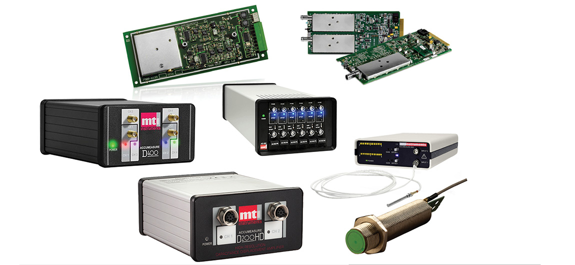
Capacitance sensors play a crucial role in semiconductor manufacturing processes for various for various applications. They are utilized for measuring and monitoring parameters such as film thickness, displacement and wafer-to-wafer uniformity.
MTI Instruments’ Accumeasure product line features capacitive sensor products for high resolution gap and displacement measurements that require a high level of accuracy that is both stable and repeatable. Capacitive measurements can be performed in a multitude of environments using non-contact passive capacitance probes that are not affected by magnetic fields, temperature, humidity, nuclear radiation or pressure.
Extremely high-precision and high linearity amplifiers make these systems ideal for critical measurements in X-Y stages, rotating spindles, shaft position,
armature gap, disk position, and piezo electric positioning applications. MTI’s Accumeasure product line delivers a highly stable, accurate, low noise amplifer with a fast response time.
PA Series
Power Analyzers
Power Analyzers
Application: Semiconductor Test & Characterization

Power analyzers are essential tools in semiconductor manufacturing for measuring and analyzing electrical power parameters of semiconductor devices, circuits, and systems. They provide valuable insights into power consumption, efficiency, and performance, enabling engineers to optimize power usage, diagnose issues, and ensure the quality of their semiconductor products. Vitrek’s precision harmonic power analyzer, the PA920 is the most accurate power analyzer available on
the market today (0.024%). The PA920’s modular design can hold up to 4 channels of power measurement in any combination of different channel card types. It is flexible, easy-to-use and provides high-performance — at a price that won’t break your budget.
The PA920 is the workhorse of power analyzers. It can operate from uW to MW. It’s six test instruments in one: 1) Power Analyzer, 2) Oscilloscope, 3) Data Logger, 4) Conducted Emissions Analyzer, 5) Spectrum Analyzer and 6) Phase Meter. It is also small, light, accurate and easy-to-use.
DL Series
Electronic DC Load
Electronic DC Load
Application: Semiconductor Test & Characterization
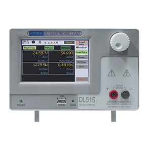
Vitrek’s DL Series of DC Electronic Load devices are the ideal choice for testing and characterizing DC power sources, power supplies, and semiconductor devices. They provide a controllable load that simulates real-world operating conditions, allowing engineers to evaluate the performance, stability, and efficiency of their designs. The DL Series is equipped with an easy-to-read color display and is a combined load, four five-digit meters, an oscilloscope and a datalogger in one compact, easy-to-use instrument.
The design utilizes high performance semiconductors with high speed and high accuracy, and wide dynamic range of loading from 10 µW to 14.5 kV. The DL Series
offers transient and non-linear loading capabilities and sweep feature. The highly accurate (0.035% base voltage and current accuracies) enables use in a wide range of applications from production line settings to the engineering bench.
.
High Speed
Digitizers
Digitizers
Application: Wafer Metrology, Test & Characterization, Fabrication
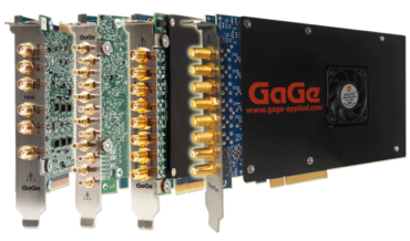
High-speed digitizers, also known as high-speed data acquisition systems or oscilloscopes, are essential tools used in semiconductor manufacturing for capturing
and analyzing fast electrical signals with high fidelity. They enable engineers to observe and measure the behavior of semiconductor devices and circuits in real-time, facilitating design validation, performance analysis, and troubleshooting.
GaGe high-performance digitizers are renowned for sustaining the maximum effective number of bits (ENOB) over a wide signal frequency range with quality signal conditioning and signal fidelity features.
With sampling rates up to 6 GS/s and very deep onboard acquisition memory of up to 16 GB, our high speed PCIe and PXIe digitizers provide optimal combinations of high sampling speeds with 8-bit, 12-bit, 14-bit, and 16-bit high resolution rates with large sampling memory options and high-speed data streaming capabilities.
Resources
Press Release: Vitrek Supports the Semiconductor Industry’s Urgent Demand for High-Performance Test Equipment Driven by the CHIPS and Science Act
The $52.7 billion legislation passed in 2022 is driving the expansion of US-based semiconductor sector; Vitrek’s product portfolio includes test and data acquisition products essential for advanced R&D and semiconductor manufacturing.
MTI Instruments Whitepaper: Capacitance Guide to Industrial Applications
Capacitance Guide to Industrial Applications This guide from MTI Instruments explains what you need to know about using electrical capacitance for measurement in industrial applications, including advanced [...]
Whitepaper: Why Capacitance? Benefits and Applications of Digital Capacitive Sensors
Industry applications illustrate the versatility and benefits of today's digital capacitive sensor technology. The electrical capacitance formed between a capacitance probe and target surface varies as a function of the distance, or gap, between those two surfaces.
CHIPS Act
CHIPS for AMERICA CHIPS: Investments in innovation, resilience, and a more competitive American future. Vitrek Supports US Semiconductor Manufacturers! Vitrek brands have supported semiconductor manufacturers like Intel, NVIDIA, Samsung, Qualcomm and others for [...]
Whitepaper: Semiconductor Wafer Measurement for Increased Productivity
Semiconductor Wafer Measurement for Increased Productivity This three-part article describes how manufacturers leverage capacitance-based inspection systems for semiconductor wafers. The article reviews best-practices, consequences of failing to inspect semiconductor wafers [...]
The Cost of Failing to Inspect Semiconductor Wafers
This is the second of three articles in Semiconductor Wafer Measurement for Increased Profitability. The first article in this series explains why disc geometry matters. The third article describes the benefits of using semi-automated, fully-automated, and manual systems for [...]
Semiconductor Industry Applications
Semiconductor Manufacturing Application Overview Vitrek offers a variety of products supporting the semiconductor industry for quality control of the fabrication process as well as testing and verification of semiconductor devices' operational performance [...]
Capacitance Sensors Facilitate 3D IC Construction
Capacitance Sensors Facilitate 3D IC Construction Semiconductor, Research & Development 3D IC Construction Distance, Positioning, Displacement Description [Application Note 70518] To boost device performance, today's [...]
Thickness Gauge Measurement With Conductive Wafers and Thin Films
Thickness Gauge Measurement With Conductive Wafers and Thin Films Consumer Electronics Electronics Parts Profiling Thickness Description Using MTI's capacitive thickness gauge Proforma 300i with conductive [...]
Semiconductor Wafer Lapping and Displacement Measurement
Semiconductor Wafer Lapping and Displacement Measurement Semiconductor Semiconductor Wafer Manufacturing Displacement Description Semiconductor Wafer Lapping and Displacement Measurement This application note explains how MTI's Accumeasure [...]
MTI’s Accumeasure HD Amplifier vs. SmarAct’s PicoScale Interferometer
MTI's Accumeasure HD Amplifier vs. SmarAct's PicoScale Interferometer Research & Development Piezoceramic, 1-3 Pzt / Polymer Composite And Pvdf Film Amplitude Description This application note [...]
Connecting Encoders to MTI’s Digital Accumeasure
Connecting Encoders to MTI's Digital Accumeasure MTI's Digital Accumeasure D has the ability to accept one or two digital quadrature encoders. The encoders can be linear slide-type or rotary. Digital [...]
Thickness and TTV of Semiconducting Wafers
Thickness and TTV of Semiconducting Wafers Semiconductor Thickness And TTV Of Semiconducting Wafers Thickness Description Introduction:  Silicon wafers are ordinarily highly conductive and easy to [...]
Lithography Optics Position Focus
Lithography Optics Position Focus Semiconductor Lithography Optics Position Focus Positioning Description One specific area where capacitance systems excel is high resolution focusing of complex lens [...]
Push-Pull Capacitance Sensor Measures Ungrounded Targets
Push-Pull Capacitance Sensor Measures Ungrounded Targets Solar, Semiconductor Measurement of Ungrounded Targets Thickness, Metrology Description [Application Note 50318] Today’s semiconductor and solar industries drive the [...]
Wafer Measurement – Ungrounded
Wafer Measurement - Ungrounded Semiconductor Wafer Measurement - Ungrounded Metrology Description MTI Instruments Inc. has developed a thickness measurement device that eliminates the effect of [...]
Wafer Thickness, Bow, Warp And TTV
Semiconductor Wafer Thickness, Bow, Warp And Ttv Surface Description Thickness Measurement ASTM F657: The distance through a wafer between corresponding points on the front [...]
Tape Cartridge Movement
Tape Cartridge Movement Semiconductor Tape Cartridge Movement Positioning Description Researchers are presently working on drives with track widths in the 5 to 1 micron region. For [...]
Wafer QA/QC After Slicing And Polishing
Wafer QA/QC After Slicing And Polishing Semiconductor Wafer Qa/Qc After Slicing And Polishing Surface Description Introduction: When wafers are sliced up with wire saws, they are [...]
Wire Bonding
Wire Bonding Semiconductor Wire Bonding Level Description Introduction:  Machine automation frequently involves measuring small distances extremely accurately. Wire Bonding is one such application with some challenging [...]
GaAs Substrate Thickness Measurement
GaAs Substrate Thickness Measurement Semiconductor Gaas Substrate Thickness Measurement Thickness Description Measuring Thickness of Wafers with Different Chemistries Introduction:  Silicon wafers are ordinarily highly conductive [...]
Photolithography Using Capacitance Sensors
Photolithography Using Capacitance Sensors Semiconductor Photolithography Using Capacitance Sensors Positioning Description When it comes to photolithography, how accurate are our sensors? Accurate enough to measure [...]
Hard Drive Position
Semiconductor Hard Drive Position Positioning Description
LED Substrate Thickness
LED Substrate Thickness Semiconductor Led Substrate Thickness Thickness Description Remember that old acronym, GIGO?  Garbage in garbage out, it can apply to raw materials as [...]
About Wafer Bow And Warp Measurement Systems
Semiconductor/Solar Wafer Bow And Warp Metrology/Surface About Wafer Bow And Warp Measurement Systems Thickness Measurement for Metrology Systems ASTM F657: The distance through a wafer between [...]
MTI Video: Wafer Inspection & Metrology Startup (Proforma 300iSA)
https://youtu.be/mawagL6Yg3U
New Video from MTI! Closed-loop System to Monitor and Control Conductive Film Thickness During Manufacturing
Closed-loop System to Monitor and Control Conductive Film Thickness During Manufacturing This animation demonstrates how Accumeasure with capacitance probes can be used as a solution to measure and control conductive film thickness in [...]
LED SUBSTRATE THICKNESS
Industry Semiconductor Applications Photolithography Using Capacitance Sensors Measurement Type Positioning Description Remember that old acronym, GIGO? Garbage in garbage out, it can apply to [...]
WAFER MEASUREMENT – UNGROUNDED
Industry Semiconductor Applications Wafer Measurement – Ungrounded Measurement Type Metrology Description MTI Instruments Inc. has developed a thickness measurement device that eliminates the effect [...]
LITHOGRAPHY OPTICS POSITION FOCUS
Industry Semiconductor Applications Photolithography Using Capacitance Sensors Measurement Type Positioning Description One specific area where capacitance systems excel is high resolution focusing of complex [...]
PHOTOLITHOGRAPHY USING CAPACITANCE SENSORS
Industry Semiconductor Applications Lithography Optics Position Focus Measurement Type Positioning Description When it comes to photolithography, how accurate are our sensors? [...]
PIEZOELECTRIC STACK MOTION
Fotonic sensors are ideal for making dynamic measurement of very small oscillatory motions. Using the MTI-2100 with a spectrum analyzer, angstrom level measurements are possible. Would you like to know more? Okay let’s set up [...]
PIEZOELECTRIC DEVICE AMPLITUDE
Measuring Piezoelectric device amplitude including piezoceramic, 1-3 PZT/polymer composite and PVDF film A “PZT ” is a piezoelectric device which generates motion when a voltage is applied across the crystal.The motion can be anywhere from [...]
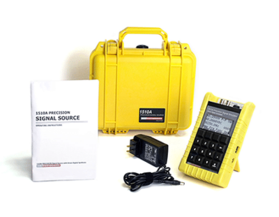
High Precision Portable Signal Generators and Calibrators: Everything You Need to Know
High precision portable signal generators are portable electronic devices that generate highly precise signals for testing, system calibration, sensor simulation, troubleshooting, and monitoring. Unlike the benchtop signal generators that are used in laboratories, these [...]
Measuring Glass wafer thickness with a Proforma 300i
Measuring glass substrate thickness with a Proforma 300i Semiconductor Glass Wafer Thickness Measurement Thickness Applications testing of glass (substrate) thickness An applications experiment was made with [...]
Contact vs. Non-Contact Measurement and Linear Displacement Sensors
Contact vs. Non-Contact Measurement and Linear Displacement Sensors Linear displacement sensors are used to measure the distance between two points or two plane surfaces. They use various technologies, but there are two basic types: [...]
Semiconductor Wafer Lapping and Displacement Measurement
Semiconductor Wafer Lapping and Displacement Measurement Semiconductor Semiconductor Wafer Manufacturing Displacement Description Semiconductor Wafer Lapping and Displacement Measurement This application note explains how MTI’s Accumeasure [...]
Measure Wafer Bow, Warp and TTV with Capacitance
The flatness of silicon wafers used to manufacture integrated circuits is controlled to tight tolerances to help ensure that the whole wafer is sufficiently flat for lithographic processing. To ensure your wafer manufacturing process [...]
Product Education & Training
Education & Training Vibration Measurement & Engine Rotor Balancing High-Speed Data Acquisition Products for Streaming Applications Industry Application Webinars Test & Measurement [...]
Common Test and Calibration Uses of the 1510A Portable Signal Generator
Powerful Ways the Portable 1510A Can Be Used In The Field As one of the most versatile and powerful hand-held signal generators on the market, the 1510A is a two-channel, battery-powered, [...]
How to Reduce Inconsistent Wafer Measurements
How to Reduce Inconsistent Wafer Measurements Avoid 5 Common Mistakes That Destroy Wafer Measurement Accuracy You take pride in your work. You’re precise, accurate [...]
Five Common Mistakes with Semiconductor Wafer Measurement
Semiconductor wafer measurement requires a high degree of precision. The right metrology equipment and inspection processes are important, but so is procedural consistency and attention to detail. If you’re not getting the results you [...]
Capacitance Guide for Industrial Applications
Accumeasure Digital Capacitance System D Series Gen 3 View Product Capacitance Displacement and Gap Measurement Probes View Product Accumeasure Analog Capacitance System View Product Basic Principles [...]
3D Integrated Circuits Use Capacitive Sensing to Ensure Coplanarity
Three-dimensional (3D) integrated circuits (ICs) feature silicon wafers and dies that are stacked vertically for improved device performance. By using the Z-axis, 3D ICs can overcome the power and footprint limitations associated with two-dimensional [...]
About Wafer Bow And Warp Measurement Systems
Semiconductor/Solar Wafer Bow And Warp Metrology/Surface About Wafer Bow And Warp Measurement Systems Thickness Measurement for Metrology Systems ASTM F657: The distance through a wafer between [...]
Laser Thickness Gauge System Principles
Microtrak™ 3 TGS The Microtrak™ 3 TGS system is specifically designed for thickness applications utilizing two lasers. The product can be used in a standalone configuration or easily interfaced with PLCs and PCs. Each module [...]


