
 Press Release: Vitrek Highlights Growing Importance of Wafer Stress Characterization for Advanced Semiconductor Manufacturing Gallery
Press Release: Vitrek Highlights Growing Importance of Wafer Stress Characterization for Advanced Semiconductor Manufacturing
Brand-MTI, Industry-Semiconductor, Industry-Semiconductor-GaGe, Industry-Semiconductor-MTI, Industry-Semiconductor-Vitrek, New & Press Releases, News-MTI, Press Releases-MTI
Press Release: Vitrek Highlights Growing Importance of Wafer Stress Characterization for Advanced Semiconductor Manufacturing
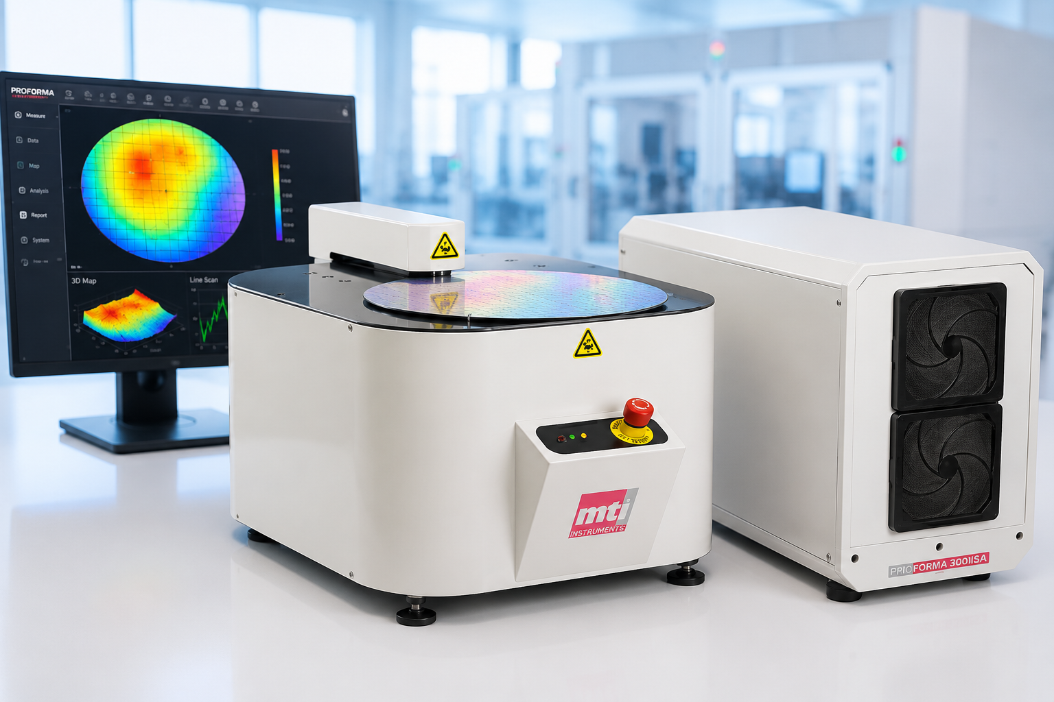
Vitrek Highlights Growing Importance of Wafer Stress Characterization for Advanced Semiconductor Manufacturing MTI Instruments Proforma™ non-contact wafer metrology systems help manufacturers optimize thin-film processes, improve process control, and increase production yield. Lockport, IL — July 28, 2026— Vitrek, a leading manufacturer of precision test and measurement equipment, highlighted the growing importance of wafer stress measurement in semiconductor manufacturing as advanced packaging, heterogeneous integration, silicon carbide (SiC), gallium nitride (GaN), MEMS, and photonics applications continue to drive demand for tighter process control, improved manufacturing consistency, and higher device reliability. As semiconductor manufacturing processes become increasingly complex, engineers are [...]
 News Release: Vitrek Highlights Critical Role of Wafer Thickness Metrology in AI and Advanced Packaging Manufacturing Gallery
News Release: Vitrek Highlights Critical Role of Wafer Thickness Metrology in AI and Advanced Packaging Manufacturing
Brand-MTI, Industry-Semiconductor, Industry-Semiconductor-GaGe, Industry-Semiconductor-MTI, Industry-Semiconductor-Vitrek, New & Press Releases, News-MTI, Press Releases-MTI
News Release: Vitrek Highlights Critical Role of Wafer Thickness Metrology in AI and Advanced Packaging Manufacturing
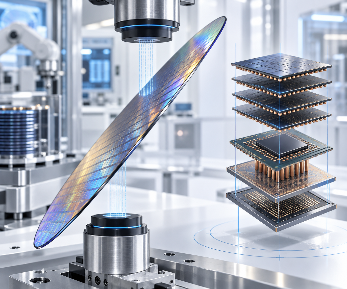
Vitrek Highlights Growing Importance of Wafer Stress Characterization for Advanced Semiconductor Manufacturing MTI Instruments Proforma systems help semiconductor manufacturers monitor backside processing for HBM, chiplets and next-generation computing devices LOCKPORT, Il — September 23, 2026 — Vitrek is highlighting the growing importance of precision wafer-thickness measurement as semiconductor manufacturers expand production of GPU/AI Engines, high-bandwidth memory, Traditional CPUs, Programmable logic, and Power Semiconductors. Advanced packaging technologies combine logic, memory, interposers and specialized dies within tightly controlled structures. To meet package-height and integration requirements, wafers often undergo backside grinding, polishing and other thinning operations. As wafers become thinner, [...]
 Press Release: Vitrek Supports the Semiconductor Industry’s Urgent Demand for High-Performance Test Equipment Driven by the CHIPS and Science Act Gallery
Press Release: Vitrek Supports the Semiconductor Industry’s Urgent Demand for High-Performance Test Equipment Driven by the CHIPS and Science Act
Brand-GaGe, Brand-MTI, Brand-Vitrek, Brands-All, Industry-Manufacturing, Industry-Semiconductor, Industry-Semiconductor-Vitrek, New & Press Releases, News-All Brands, News-Events, News-GaGe, News-Industry, News-MTI, News-Vitrek, Press Releases-Vitrek
Press Release: Vitrek Supports the Semiconductor Industry’s Urgent Demand for High-Performance Test Equipment Driven by the CHIPS and Science Act
The $52.7 billion legislation passed in 2022 is driving the expansion of US-based semiconductor sector; Vitrek’s product portfolio includes test and data acquisition products essential for advanced R&D and semiconductor manufacturing.