CHIPS Act
CHIPS for AMERICA CHIPS: Investments in innovation, resilience, and a more competitive American future. Vitrek Supports US Semiconductor Manufacturers! Vitrek brands have supported semiconductor manufacturers like Intel, NVIDIA, Samsung, Qualcomm and others for over 20 years via our test and measurement solutions. What is the CHIPS Act? The CHIPS Act, or the Creating Helpful Incentives to Produce Semiconductors for America's Future Act, is a pivotal piece of legislation in the United States aimed at bolstering domestic semiconductor manufacturing. Introduced in 2021, it represents a bipartisan effort to address the growing global [...]

Semiconductor Industry Applications
Semiconductor Industry Applications Vitrek offers a variety of products supporting the semiconductor industry for quality control of the fabrication process as well as testing and verification of semiconductor devices' operational performance as well as supporting the performance of capital equipment use in the semiconductor manufacturing process. Some Vitrek product applications include: Semiconductor Wafer Metrology Monitoring wafers during preparation stages to check thickness for compliance with minimal bow, warp and total thickness variation (TTV). In-process monitoring of solar/photovoltaic wafer measuring for multi-channel thickness, TTV & bow measurement. Ultrasonic, non-destructive inspection of wafers for potential flaws [...]
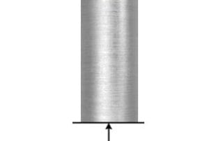
LED SUBSTRATE THICKNESS
Industry Semiconductor Applications Photolithography Using Capacitance Sensors Measurement Type Positioning Description Remember that old acronym, GIGO? Garbage in garbage out, it can apply to raw materials as well as programming. Sapphire wafers need to be of a certain quality to ensure maximum yield. Excessive TTV, Bow, and Warp lead to premature LED failure. LED manufacturers need to inspect incoming wafers. Wafer producers also need to check and control TTV, Bow and Warp. The market for sapphire wafers, driven by the growth in LED manufacturing, is booming. While the price [...]
WAFER QA/QC AFTER SLICING AND POLISHING
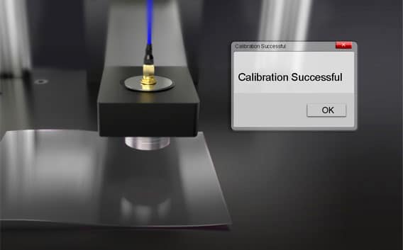
Industry Semiconductor Applications Wafer Qa/Qc After Slicing And Polishing Measurement Type Surface Description When wafers are sliced up with wire saws, they are measured to make sure they are within the specified thickness, with minimal bow, warp, and TTV. After initial measurement, they are sorted and sent for polishing. Since polishing removes material and smoothes out the rough surfaces they need to be measured again to ensure they meet thickness guidelines and quality standards. Solution: MTI Instruments manufactures multiple systems to perform thickness measurements. From semi automated Proforma 300SA to manual wafer [...]
ABOUT WAFER BOW AND WARP MEASUREMENT SYSTEMS
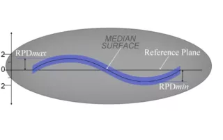
Thickness Measurement for Metrology Systems ASTM F657: The distance through a wafer between corresponding points on the front and back surface. Thickness is expressed in microns or mils (thousandths of an inch). Total Thickness Variation (TTV) ASTM F657: The difference between the maximum and minimum values of thickness encountered during a scan pattern or series of point measurements. TTV is expressed in microns or mils (thousandths of an inch). ASTM F534 3.1.2: The deviation of the center point of the median surface of a free, unclamped wafer from the median [...]

LITHOGRAPHY OPTICS POSITION FOCUS
Industry Semiconductor Applications Photolithography Using Capacitance Sensors Measurement Type Positioning Description One specific area where capacitance systems excel is high resolution focusing of complex lens systems such as those found in atomic force microscopes, vision inspection machines and photolithography tools. In a multi-million dollar photolithography tool, high accuracy, nanometer resolution and maximum thermal stability are absolutely critical to maintain proper focus and obtain integrated circuit line widths as small as 45 nanometers. Additionally, most systems demand low power consumption and maximum heat dissipation to eliminate any adverse affects from [...]
GAAS SUBSTRATE THICKNESS MEASUREMENT
Industry Semiconductor Applications Gaas Substrate Thickness Measurement Measurement Type Thickness Description Measuring Thickness of Wafers with Different Chemistries Introduction: Silicon wafers are ordinarily highly conductive and easy to measure with standard capacitive displacement sensors (See MTI’s Proforma 300i). Measuring the thickness of GaAs wafers that have high bulk resistivity (>10k Ohm/cm) is a little more difficult because the wafers act as non-conductive insulators in a capacitive sensor’s measuring field. Fortunately, MTI has a solution to this problem. Solution: It’s possible to measure the thickness and TTV of high resistivity semiconducting wafers (like GaAs) using non-contact capacitive [...]
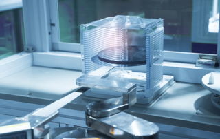
 Press Release: MTI’s Proforma 300iSA Combines SEMI and ASTM Standard Compliance in Space-Efficient Benchtop Design Gallery
Press Release: MTI’s Proforma 300iSA Combines SEMI and ASTM Standard Compliance in Space-Efficient Benchtop Design
Industry-Semiconductor-MTI, New & Press Releases, News, News-MTI-Instrumentation, Press Releases, Press Releases-MTI
Press Release: MTI’s Proforma 300iSA Combines SEMI and ASTM Standard Compliance in Space-Efficient Benchtop Design
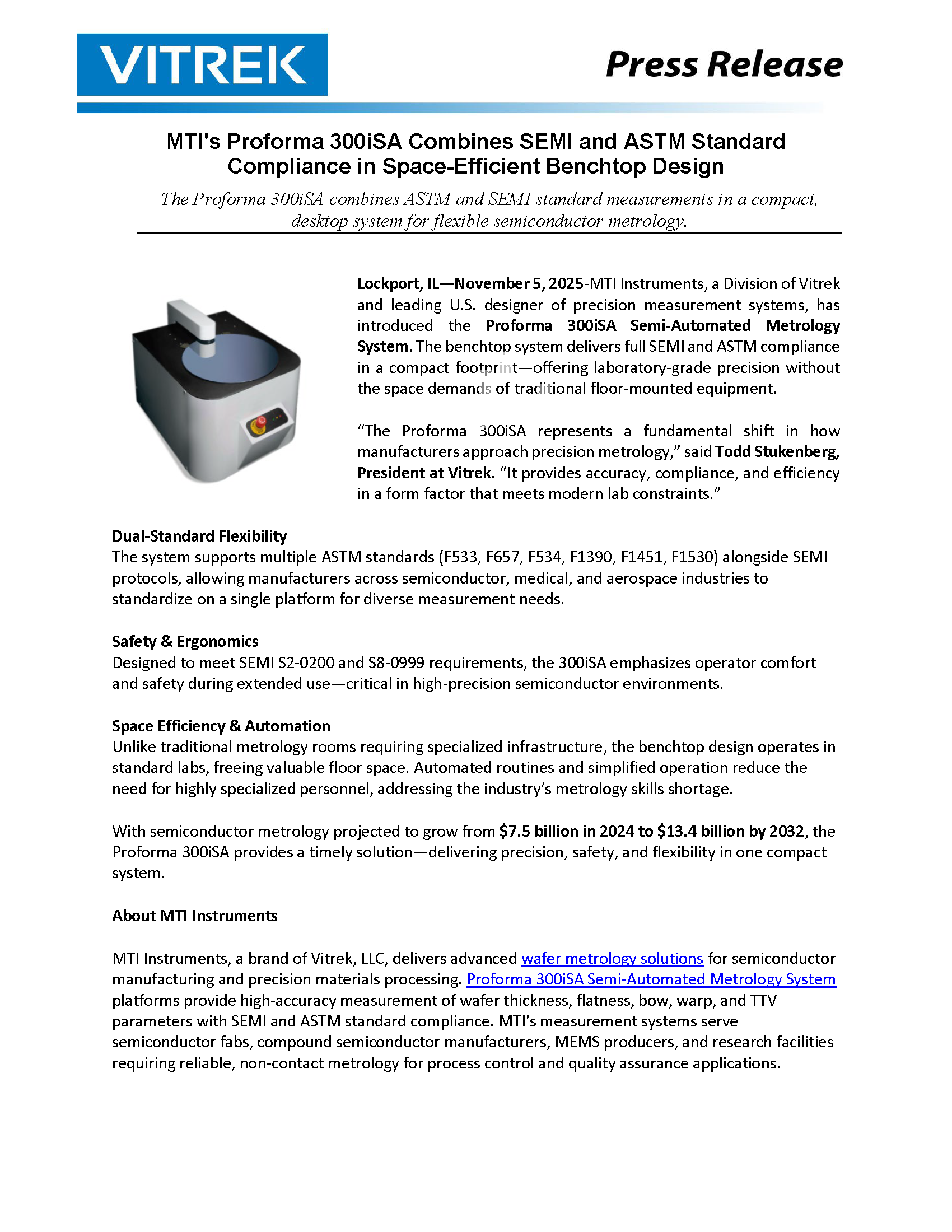
MTI's Proforma 300iSA Combines SEMI and ASTM Standard Compliance in Space-Efficient Benchtop Design The Proforma 300iSA combines ASTM and SEMI standard measurements in a compact, desktop system for flexible semiconductor metrology. Lockport, IL, November 18, 2025 – Vitrek, a leading U.S. designer of precision measurement systems, has introduced the MTI Instruments Proforma 300iSA Semi-Automated Metrology System. The benchtop system delivers full SEMI and ASTM compliance in a compact footprint—offering laboratory-grade precision without the space demands of traditional floor-mounted equipment. “The Proforma 300iSA represents a fundamental shift in how manufacturers approach precision metrology,” said Todd Stukenberg, President at [...]
 Compliance Testing of Harmonic Current Emissions According to IEC61000-3-2 and IEC61000-3-12. Gallery
Compliance Testing of Harmonic Current Emissions According to IEC61000-3-2 and IEC61000-3-12.
Application Notes-Vitrek, Brand-Vitrek, Industry-Automotive, Industry-Compliance Testing, Industry-Consumer Products, Industry-Energy, Industry-Manufacturing, Industry-Medical, Industry-Medical, Industry-OEM, Industry-R&D, Industry-Semiconductor, News-All Brands, Products-Vitrek-Power-Analyzer
Compliance Testing of Harmonic Current Emissions According to IEC61000-3-2 and IEC61000-3-12.
Compliance Testing of Harmonic Current Emissions According to IEC61000-3-2 and IEC61000-3-12. Using the Vitrek PA900 Precision Harmonic Power Analyzer Introduction Compliance with electromagnetic compatibility (EMC) standards is mandatory for electrical and electronic equipment sold in many global markets. Among these, the IEC61000-3-2 and IEC61000-3-12 standards specify limits for harmonic current emissions of equipment connected to low-voltage public supply systems. These limits ensure that individual devices do not contribute excessively to harmonic distortion on the power grid, which can lead to overheating in transformers, nuisance tripping of breakers, and interference with other equipment. The Vitrek PA900 Precision Power [...]
 Power Analyzers: The Backbone of Modern Electrical Engineering Gallery
Power Analyzers: The Backbone of Modern Electrical Engineering
Brand-Vitrek, Industry-Automotive, Industry-Compliance Testing, Industry-Consumer Products, Industry-Energy, Industry-Manufacturing, Industry-Medical, Industry-Medical, Industry-OEM, Industry-R&D, Industry-Semiconductor, News-All Brands, Products-Vitrek-Power-Analyzer, Whitepapers-Vitrek
Power Analyzers: The Backbone of Modern Electrical Engineering
Introduction In the fast-paced world of electrical engineering, ensuring accurate power measurement is crucial for efficiency, reliability, and compliance. Power analyzers play a key role in industries ranging from renewable energy to semiconductor manufacturing, providing engineers with the insights needed to optimize performance and troubleshoot electrical systems. At the forefront of this technology is Vitrek, a leading provider of high-accuracy power analyzers designed for demanding applications. The Role of Power Analyzers in Engineering Power analyzers measure critical electrical parameters such as voltage, current, power factor, and harmonic distortion. Unlike basic meters, these advanced instruments offer high precision measurements over [...]