
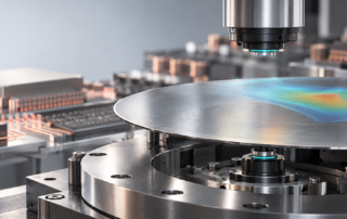
Application Note: Monitoring Wafer Thickness During Backside Processing for AI and Advanced Packaging
Introduction AI accelerators, high-performance computing systems, high bandwidth memory and chiplet-based devices increasingly rely on 2.5D and 3D advanced packaging processes that combine logic, memory, interposers and specialized dies within tightly controlled structures. Before stacking or bonding, wafers may undergo coarse grinding, fine grinding, polishing and other backside processes. These operations must remove substantial material while maintaining the thickness and geometry required by the package design. This application note explains how the MTI Instruments Proforma 300i and Proforma 300iSA can be used at defined process checkpoints to verify wafer thickness, evaluate uniformity and identify process changes before wafers proceed [...]
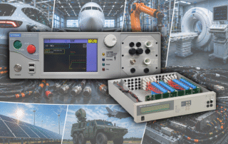 Whitepaper: The Future of Cable Testing: Why Intelligent Automation is Replacing Manual Validation Gallery
Whitepaper: The Future of Cable Testing: Why Intelligent Automation is Replacing Manual Validation
Brand-Vitrek, Industry-Aerospace, Industry-Automotive, Industry-Cable Test, Industry-Compliance Testing, Industry-Consumer Products, Industry-Electronics, Industry-Government/Military, Industry-Lighting, Industry-Manufacturing, Industry-Medical, New & Press Releases, Whitepapers-Vitrek
Whitepaper: The Future of Cable Testing: Why Intelligent Automation is Replacing Manual Validation
Introduction Cable assemblies are evolving rapidly as products become more compact, more powerful, and more connected. Today’s designs often operate at higher voltages while fitting into smaller packaging envelopes, forcing engineers to balance electrical performance with limited physical space. At the same time, many assemblies now include a greater number of conductors and increasingly combine mixed signal and power paths within a single harness. Environmental demands are also rising. Cable systems may need to withstand vibration, temperature extremes, moisture, chemicals, or continuous motion depending on the application. Alongside these technical requirements, manufacturers face growing expectations for stronger quality documentation [...]
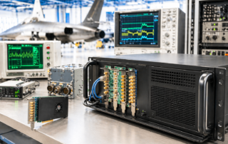
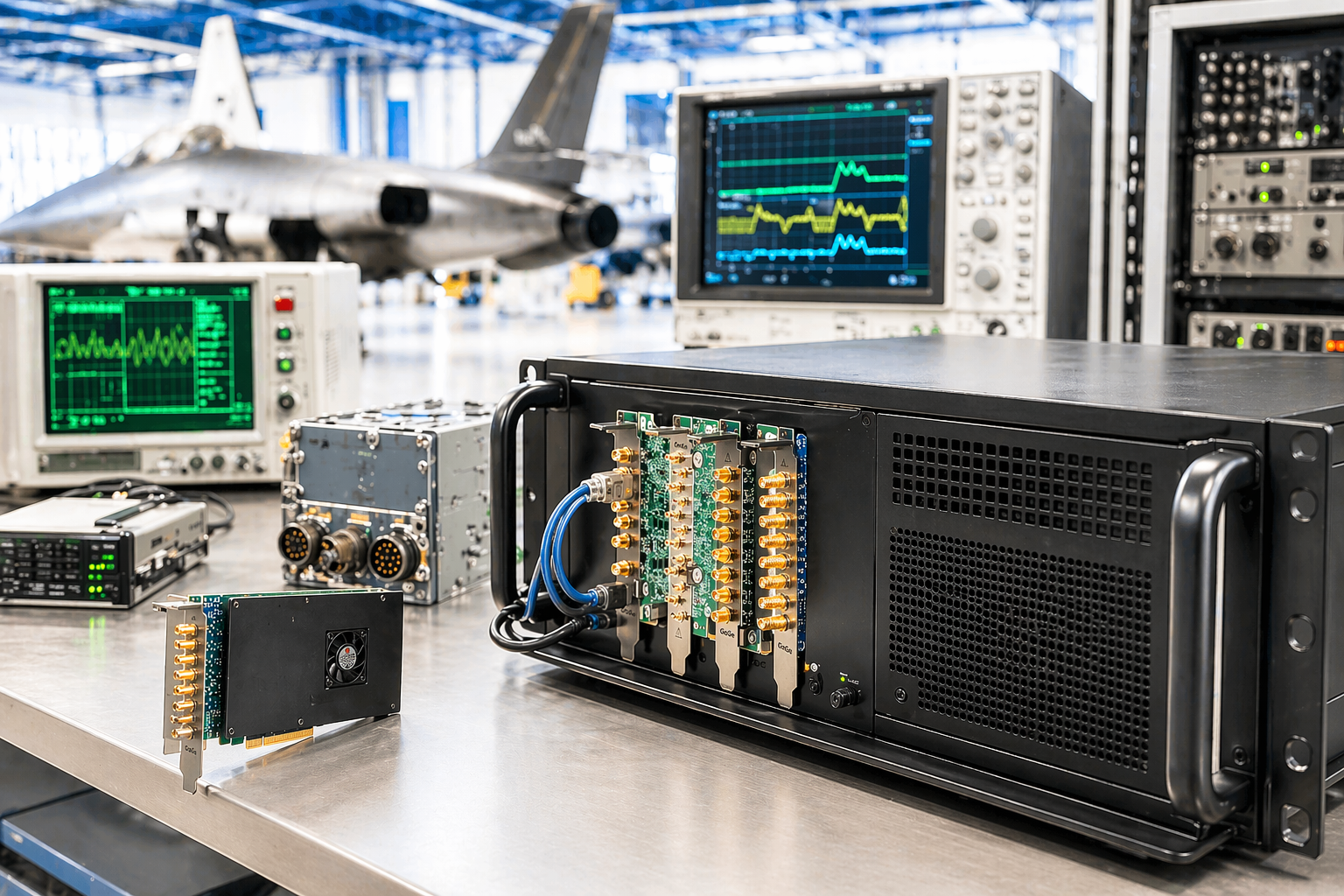
Application Note: Modernizing a Legacy Military Avionics Test System with a Programmable GaGe High-Speed Digitizer
Introduction Across military and aerospace maintenance operations, many proven test systems remain in service decades after their original deployment. These systems often support critical certification procedures, validated workflows, and platform-specific compliance tests that are costly or impractical to replace. While the airframes and missions may evolve, the test infrastructure built around them often remains indispensable. The challenge arises when key instruments inside those systems become obsolete. Aging oscilloscopes, digitizers, controllers, and interface hardware can create maintenance burdens, calibration issues, and long-term support risks. Replacing them is rarely simple. In regulated or mission-critical environments, a modern instrument must not only [...]
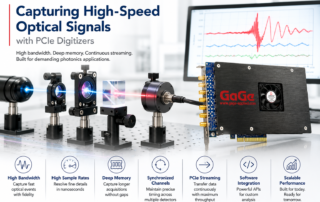
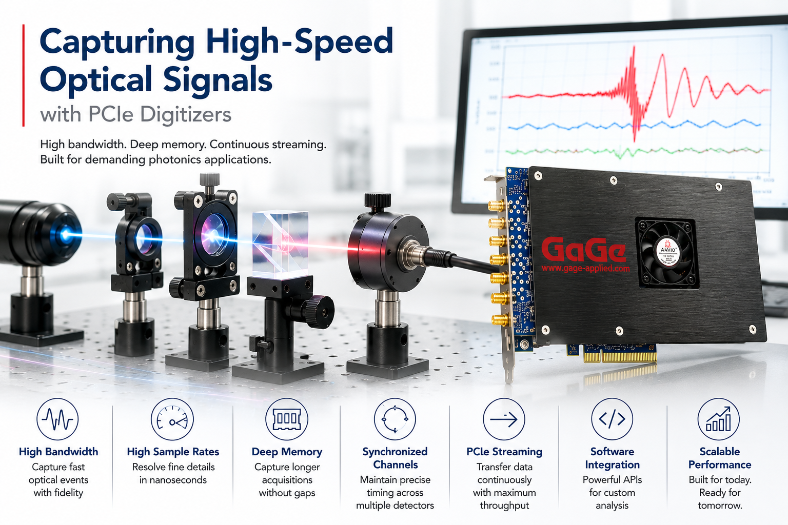
Application Note: Improving Optical Measurements Through High-Speed Data Acquisition
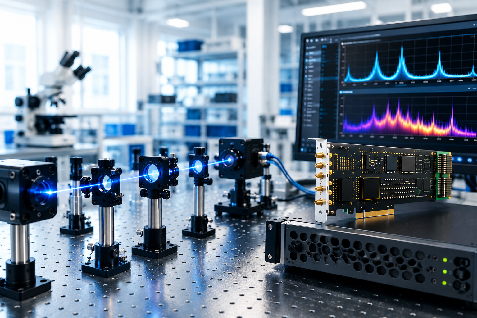
Introduction Advances in optical engineering are driving the need for faster, more accurate data acquisition systems. Whether characterizing laser pulses, measuring fiber optic sensors, or analyzing highspeed optical communications, today’s photonics applications generate electrical signals that demand exceptional sampling performance and timing accuracy. While the optical source may be light, the measurement ultimately depends on capturing an electrical waveform produced by a photodiode or other optical detector. Preserving the integrity of that waveform is critical, as lost detail or timing errors can directly affect measurement accuracy, image quality, or system performance. High-speed PCIe digitizers provide the bandwidth, memory depth, [...]
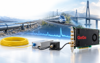
Technology Brief: GaGe Digitizers — Powering the Next Generation of Distributed Fiber Sensing
Introduction An exciting new technology called Distributed Fiber Optic Sensing (DFOS) transforms ordinary communications fiber into a continuous sensing array that extends over kilometers. Communications fiber is designed to minimize optical attenuation and maximize the transmitted optical signal. Nonetheless, a small amount of light is backscattered towards the light source. This backscatter is routinely acquired by Optical Time-Domain Reflectometers (OTDRs) to characterize fiber. Modern communications fiber typically has a very low attenuation of about 0.2 dB/km. DFOS instruments similar to OTDRs are generally called interrogators. Backscatter is divided into two types. Elastic backscatter occurs at the same energy (or, [...]
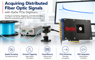
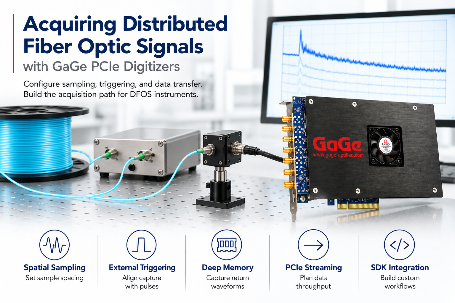
Application Note: GaGe Digitizers — Configuring GaGe Digitizers for Distributed Fiber Optic Sensing (DFOS)
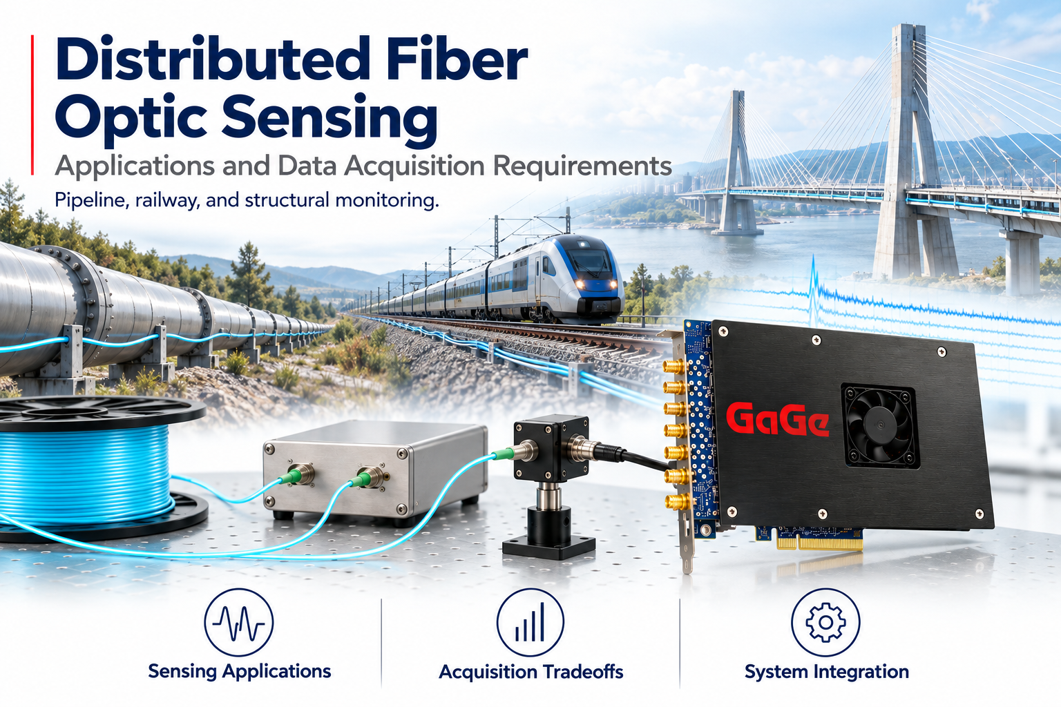
Introduction Distributed fiber optic sensing (DFOS) uses optical fiber to measure temperature, strain, or vibration at many locations along its length. By analyzing changes in backscattered light, a DFOS interrogator can monitor conditions across extended assets such as pipelines, bridges, and railway infrastructure. In pulse-based systems, the arrival time of the returned light identifies its position along the fiber, while the optical sensing method determines which physical quantities can be measured. A photodetector converts the returning light into an electrical waveform, which a high-speed digitizer captures for processing. Selecting and configuring the digitizer requires attention to sampling rate, input [...]
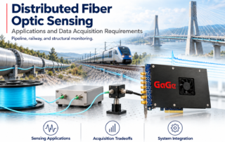
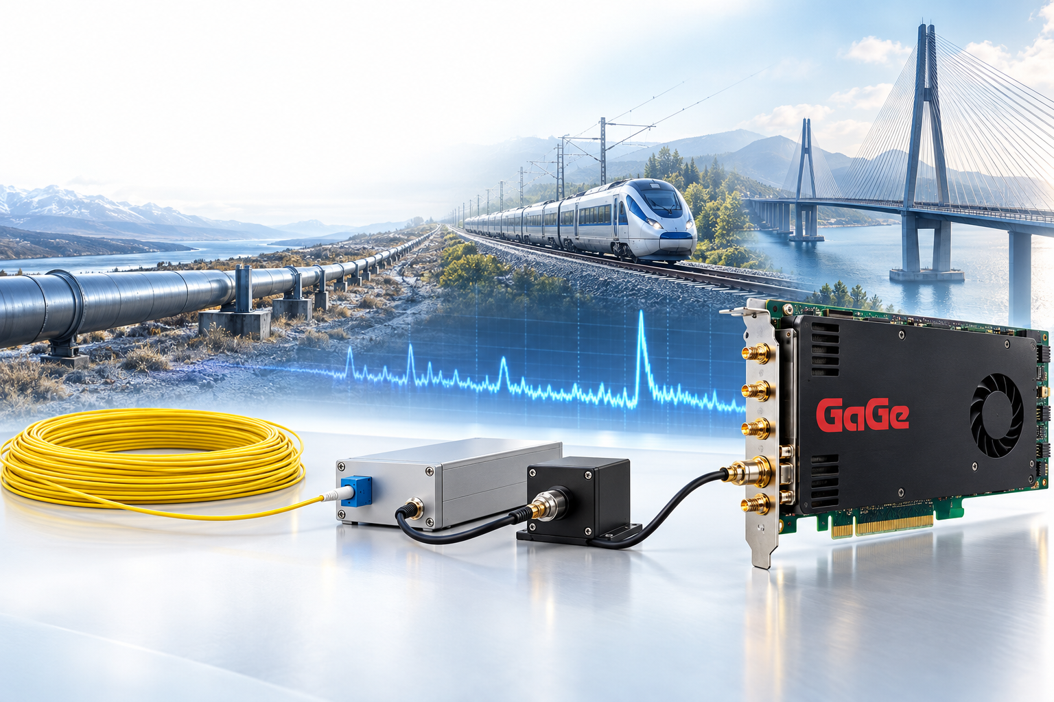
Whitepaper: Distributed Fiber Optic Sensing DFOS
Introduction Distributed fiber optic sensing (DFOS) uses optical fiber to measure temperature, strain, or vibration at many locations along a sensing path. It provides spatial information across extended assets, supporting applications such as pipeline monitoring, railway monitoring, and structural assessment. Each application places different demands on sensing range, response speed, spatial detail, and measurement reliability. For instrument developers, these needs guide the selection of the optical architecture and electrical acquisition system. A digitizer captures the output of the optical detection system, with sampling rate, bandwidth, input noise, timing, channel configuration, memory, and transfer performance influencing the information available for [...]
Whitepaper: Choosing the Right Data Acquisition Architecture for Photonics Applications
Introduction Photonics has become one of the fastest-growing fields in engineering, enabling advances in autonomous vehicles, optical communications, medical imaging, aerospace, semiconductor manufacturing, and quantum technologies. As these systems continue to evolve, engineers are challenged to capture increasingly complex optical signals while maintaining exceptional measurement accuracy, repeatability, and timing precision. At the heart of every optical measurement system is a detector that converts light into an electrical signal. The quality of the resulting data depends not only on the detector itself, but also on the architecture used to acquire, process, and analyze that signal. Selecting the appropriate data acquisition [...]
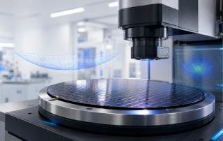
Application Note: Wafer & Thin-Film Stress Characterization Using the Proforma 300iSA
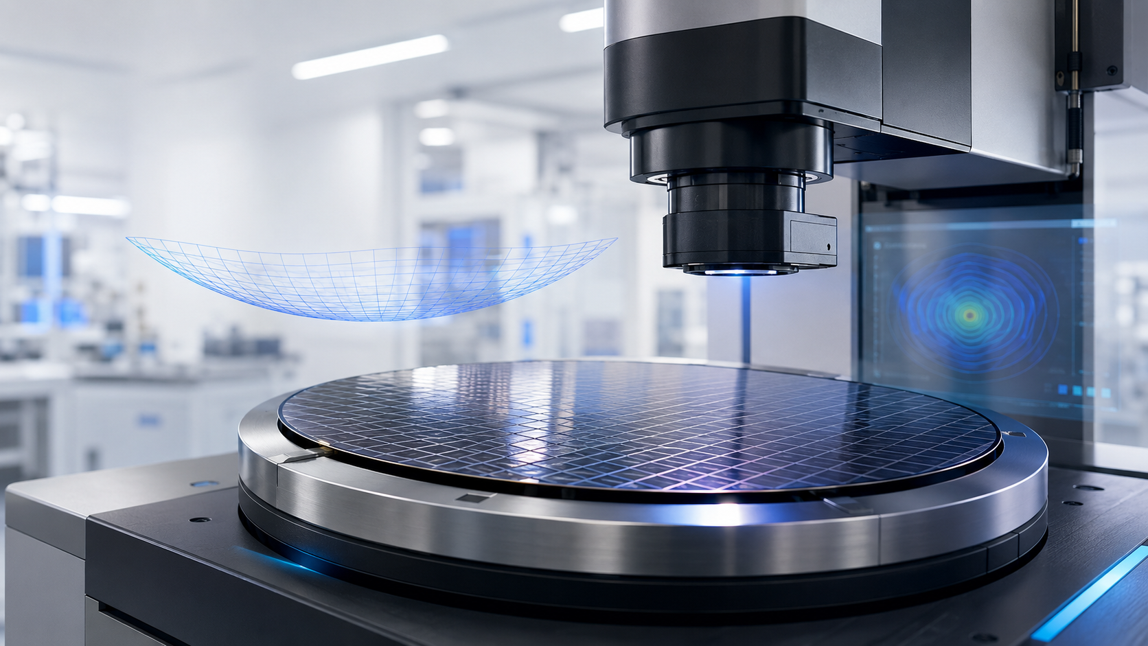
Introduction Thin films are essential to modern semiconductor devices, but every deposited, grown, bonded, or processed layer can introduce mechanical stress into the wafer. When that stress becomes excessive or inconsistent, the effects can extend well beyond the deposition step—contributing to wafer bow, cracking, delamination, overlay error, handling problems, yield loss, and downstream process instability. The MTI Instruments Proforma™ 300iSA semi-automated metrology system provides the full-wafer thickness and shape data needed to evaluate these risks. By measuring wafer geometry before and after a process step, engineers can quantify curvature change and use established film-stress relationships to calculate and trend [...]
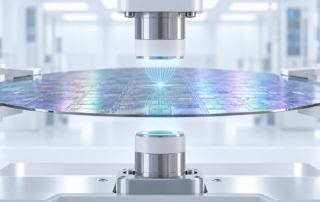
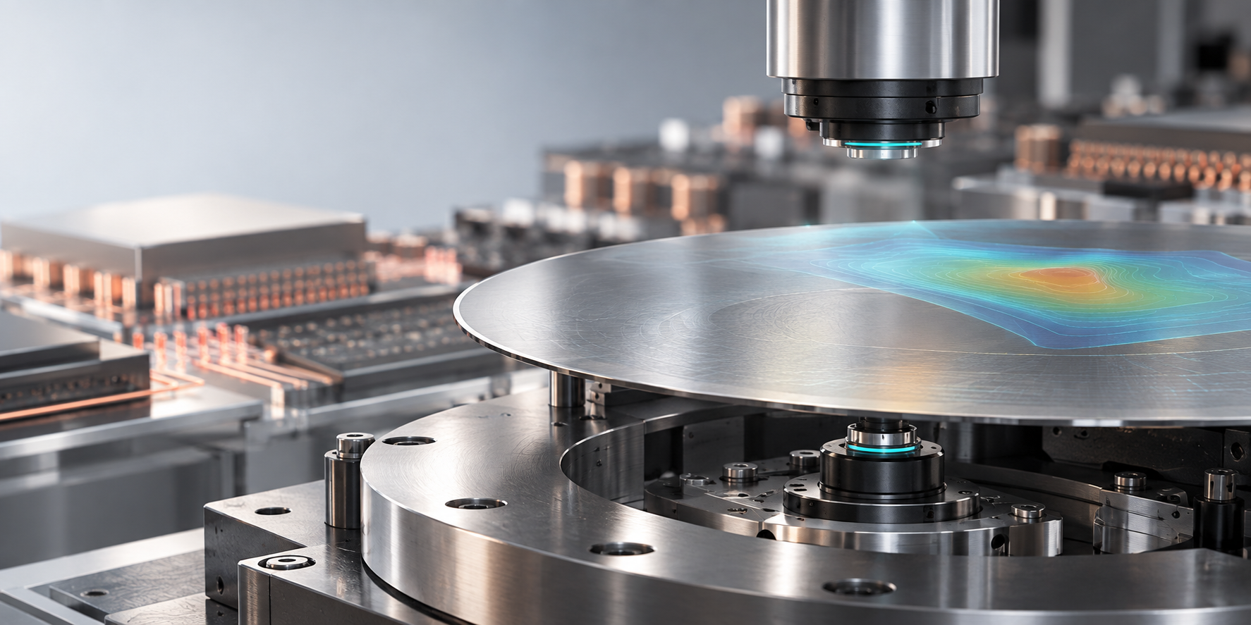
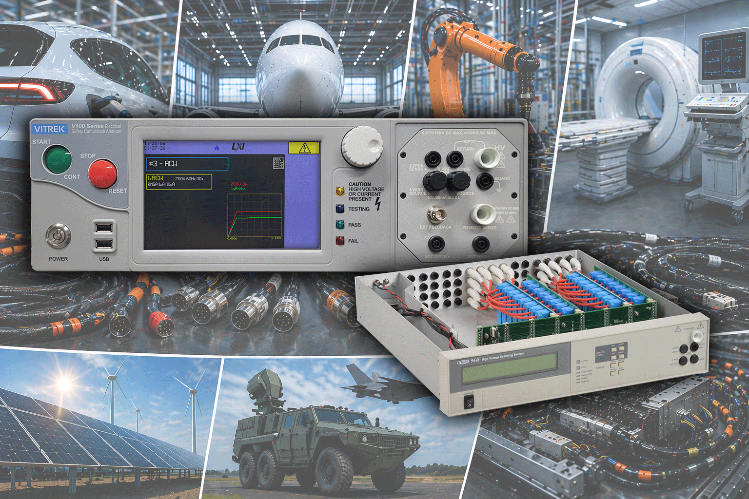
Whitepaper: Thickness Metrology for AI Accelerators, HBM and Chiplet-Based Advanced Packaging
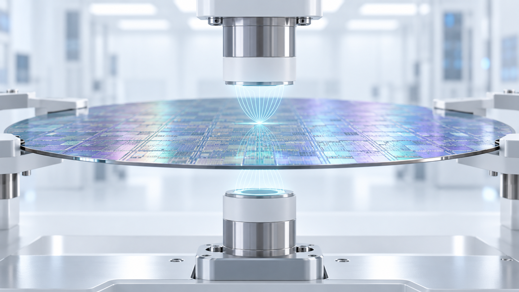
Introduction Artificial intelligence and high-performance computing are reshaping semiconductor design and manufacturing. Instead of relying exclusively on increasingly large monolithic devices, manufacturers are integrating logic, memory and specialized functions through chiplets, 2.5D packaging, 3D stacking and high-bandwidth memory. These architectures improve computing density, bandwidth and energy efficiency, but they also place greater demands on wafer thinning and backside processing. Individual wafers and dies may need to be made significantly thinner before stacking, bonding or package assembly. As thickness decreases, however, wafers become more susceptible to breakage, warpage, handling damage and non-uniform material removal. Thickness metrology therefore becomes more than [...]