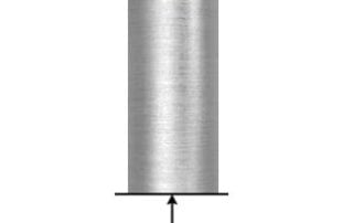
LED SUBSTRATE THICKNESS
Industry Semiconductor Applications Photolithography Using Capacitance Sensors Measurement Type Positioning Description Remember that old acronym, GIGO? Garbage in garbage out, it can apply to raw materials as well as programming. Sapphire wafers need to be of a certain quality to ensure maximum yield. Excessive TTV, Bow, and Warp lead to premature LED failure. LED manufacturers need to inspect incoming wafers. Wafer producers also need to check and control TTV, Bow and Warp. The market for sapphire wafers, driven by the growth in LED manufacturing, is booming. While the price [...]
 Whitepaper: The Future of Cable Testing: Why Intelligent Automation is Replacing Manual Validation Gallery
Whitepaper: The Future of Cable Testing: Why Intelligent Automation is Replacing Manual Validation
Brand-Vitrek, Industry-Aerospace, Industry-Automotive, Industry-Cable Test, Industry-Compliance Testing, Industry-Consumer Products, Industry-Electronics, Industry-Government/Military, Industry-Lighting, Industry-Manufacturing, Industry-Medical, New & Press Releases, Whitepapers-Vitrek
Whitepaper: The Future of Cable Testing: Why Intelligent Automation is Replacing Manual Validation
Introduction Cable assemblies are evolving rapidly as products become more compact, more powerful, and more connected. Today’s designs often operate at higher voltages while fitting into smaller packaging envelopes, forcing engineers to balance electrical performance with limited physical space. At the same time, many assemblies now include a greater number of conductors and increasingly combine mixed signal and power paths within a single harness. Environmental demands are also rising. Cable systems may need to withstand vibration, temperature extremes, moisture, chemicals, or continuous motion depending on the application. Alongside these technical requirements, manufacturers face growing expectations for stronger quality documentation [...]
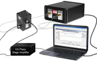
PIEZO STAGE POSITIONING
Industry Consumer Electronics Applications Piezo Stage Measurement Type Positioning Description Positioning stages using piezoelectric stack actuators (PEA) have very high resolution. However, it is difficult to achieve precise dynamic motion tracking using traditional linear controllers such as PID due to the inherent hysteresis nonlinearity of piezoelectric materials and the phase lag associated with such controllers. Capacitance Sensors are ideal for measuring the actual piezo stage position and correcting for the inherent nonlinearity through closed loop feedback. They have the stability, bandwidth and high resolution needed to do the job. [...]
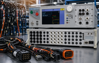 Automating Complex Cable Testing with the Vitrek V10X and 964i Gallery
Automating Complex Cable Testing with the Vitrek V10X and 964i
Application Notes-Vitrek, Brand-Vitrek, Industry-Aerospace, Industry-Automotive, Industry-Cable Test, Industry-Compliance Testing, Industry-Consumer Products, Industry-Electronics, Industry-Government/Military, Industry-Lighting, Industry-Manufacturing, Industry-Medical, Whitepapers-Vitrek
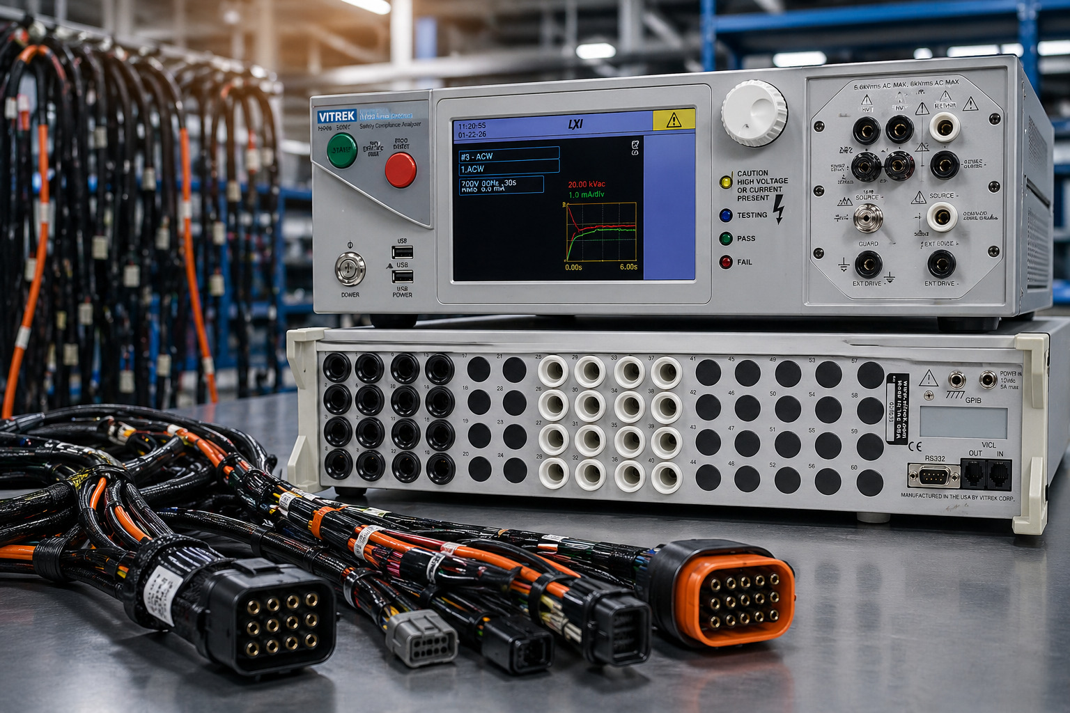
Automating Complex Cable Testing with the Vitrek V10X and 964i
Introduction Cable assemblies are no longer simple pass/fail products. Modern harnesses may contain dozens—or hundreds—of conductors, shielding paths, insulation systems, and termination points. Testing them manually is slow, labor intensive, and prone to inconsistency. The combination of the Vitrek V10X Hipot Tester and Vitrek 964i High Voltage Switching System creates a modern automated platform for validating cable safety and integrity with higher speed and repeatability. The Challenge Manufacturers of advanced cable assemblies are under constant pressure to improve quality while keeping production moving. Many products now use large pin-count connectors and complex multi-conductor designs that require access to numerous [...]
GAAS SUBSTRATE THICKNESS MEASUREMENT
Industry Semiconductor Applications Gaas Substrate Thickness Measurement Measurement Type Thickness Description Measuring Thickness of Wafers with Different Chemistries Introduction: Silicon wafers are ordinarily highly conductive and easy to measure with standard capacitive displacement sensors (See MTI’s Proforma 300i). Measuring the thickness of GaAs wafers that have high bulk resistivity (>10k Ohm/cm) is a little more difficult because the wafers act as non-conductive insulators in a capacitive sensor’s measuring field. Fortunately, MTI has a solution to this problem. Solution: It’s possible to measure the thickness and TTV of high resistivity semiconducting wafers (like GaAs) using non-contact capacitive [...]

Spindle Run Out
Industry Automotive Applications Spindle Run Out Measurement Type Positioning Description Rotating targets frequently have an intermittent, uncertain or nonexistent ground path. This introduces unwanted noise, instability, drift and reduces accuracy of the measurement. MTI Instruments offers a unique “Push-Pull” capacitance measurement system that does not require a grounded target. It utilizes two probes, built into one body, that work together to complete the ground path. One probe pushes current into the brake rotor while the adjacent probe pulls the current out. The result is a “clean”, consistent electrical sensing path. As the [...]
CAPACITANCE SENSORS FACILITATE 3D IC CONSTRUCTION
[Application Note 70518] To boost device performance, today’s semiconductor and microelectronics manufacturers are building three-dimensional integrated circuits featuring vertically-stacked silicon wafers and dies. The rationale is simple. Exploiting the Z-axis avoids the power and footprint penalties associated with two-dimensional processes. Implementing the rationale, however, is not so simple. Going vertical requires coplanar surfaces to make contact with all pins, pads, and pillars. Problem Typically, manufacturers measure the angle and gap between two planes to determine coplanarity. Bonding tool actuators rely on these angle/gap measurements to adjust components and make sure all device pins and/or solder balls reside on the [...]
MONITOR ROLLER GAPS AND PARALLELISM
Easy Roller Gap Measurement Ensures Calendering Success Many roll-to-roll finishing processes typically use a calender, or series of hard pressure rollers, to deliver smooth, high-quality products of plastic, textile, or paper (Fig 1). Ensuring a consistent material thickness, however, depends on the ability to monitor, and maintain, a precise gap between rollers. This application note describes a quick and easy means for roller gap measurement. Problem Establishing a roller gap and checking for parallelism across roller width can be a slow and cumbersome procedure. Manual measurement requires multiple sized feeler gauges which can introduce errors. Misinterpreting feeler gauge drag, [...]
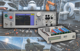
 Choosing the Right Hipot Platform for Modern Manufacturing Electrical Safety Testing Gallery
Choosing the Right Hipot Platform for Modern Manufacturing Electrical Safety Testing
Articles-Vitrek, Industry-Automotive, Industry-Battery, Industry-Cable Test, Industry-Compliance Testing, Industry-Consumer Products, Industry-Electronics, Industry-Government/Military, Industry-Lighting, Industry-Manufacturing, Industry-Medical, Industry-R&D, Knowledge Center-Vitrek, New & Press Releases, Whitepapers-Vitrek
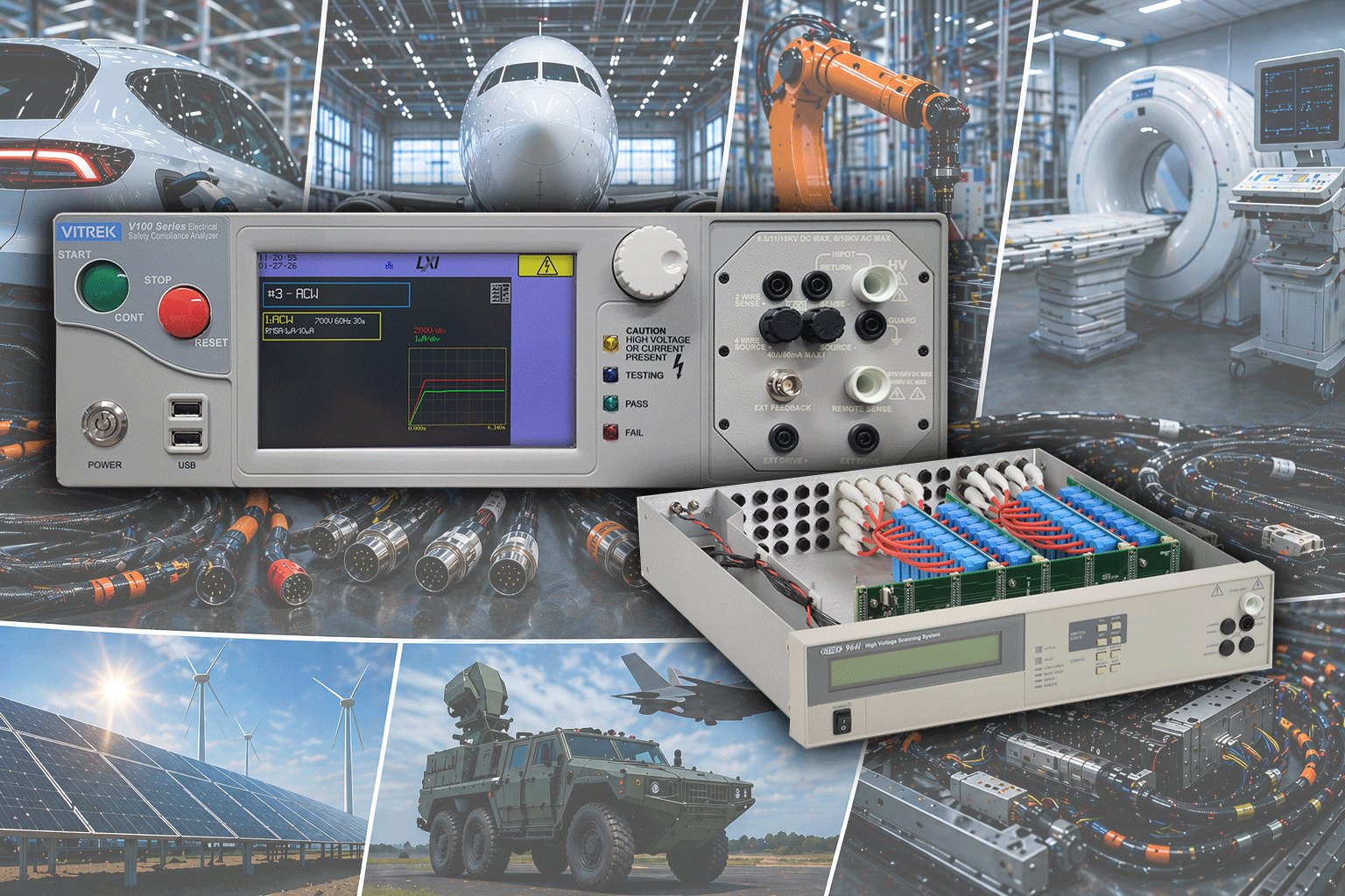
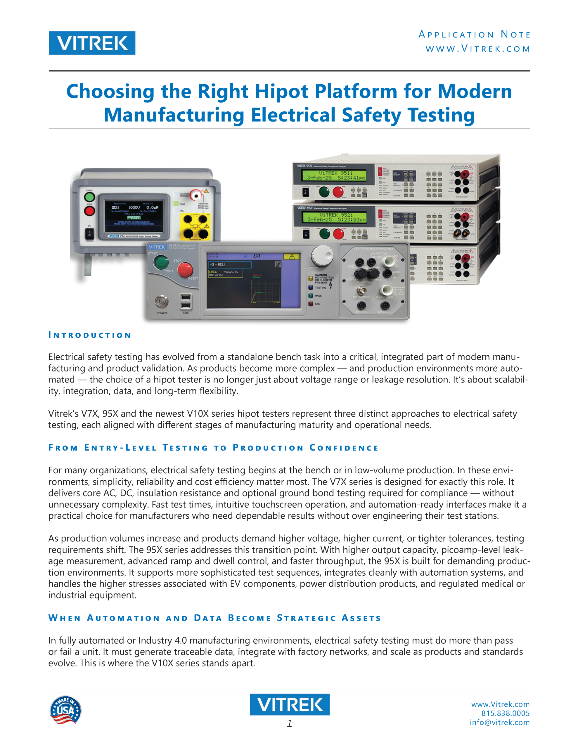
Choosing the Right Hipot Platform for Modern Manufacturing Electrical Safety Testing
Introduction Electrical safety testing has evolved from a standalone bench task into a critical, integrated part of modern manufacturing and product validation. As products become more complex — and production environments more automated — the choice of a hipot tester is no longer just about voltage range or leakage resolution. It’s about scalability, integration, data, and long-term flexibility. Vitrek’s V7X, 95X and the newest V10X series hipot testers represent three distinct approaches to electrical safety testing, each aligned with different stages of manufacturing maturity and operational needs. From Entry-Level Testing to Production Confidence For many organizations, electrical safety testing [...]

Windshield Manufacturing
Industry Automotive Applications Oil Film Measurement Type Level Description In order to maintain proper profile and thickness within a glass furnace the extrusion plate spacing must be maintained at a predetermined gap. Unfortunately, due to process changes and temperature swings this gap can fluctuate significantly in short periods of time. This variation causes the glass thickness to change (check out our glass thickness measurement devices to accurately measure thickness), producing uneven temperature gradients and creating potentially weak glass panels. To control this critical parameter the manufacturing process requires automated active feedback [...]