

Semiconductor Wafer Lapping and Displacement Measurement
Introduction This application note explains how MTI's Accumeasure technology was used with a lapping machine to measure displacement (wafer material removal) and determine the new semiconductor wafer thickness. Changes in electrical capacitance (displacement) were measured and then directly converted into a 24-bit digital reading to obtain precise digital thickness measurements. During lapping, a wafer of known start thickness is placed on a rotary lapping table. The backside of the wafer faces downward and toward a lapping surface that rotates and removes unwanted material. The amount of material that is removed varies by device type, and the entire semiconductor [...]
 MTI’s Accumeasure HD Amplifier vs. SmarAct’s PicoScale Interferometer Gallery
MTI’s Accumeasure HD Amplifier vs. SmarAct’s PicoScale Interferometer
App Notes, Application Notes-MTI, Applications, Brand-MTI, Brands, Editorials, Industry, Industry-R&D, Industry-Semiconductor, Industry-Semiconductor-MTI, Z-REPUB, z1
MTI’s Accumeasure HD Amplifier vs. SmarAct’s PicoScale Interferometer
MTI's Accumeasure HD Amplifier vs. SmarAct's PicoScale Interferometer Research & Development Piezoceramic, 1-3 Pzt / Polymer Composite And Pvdf Film Amplitude Description This application note compares MTI's Accumeasure HD amplifier to SmarAct's Picoscale interferometer in terms of resolution and accuracy for very small displacement measurements. Specifically, this comparison focuses on minimum expected resolution and the effects of noise on accuracy. High resolution interferometers are widely regarded as the instrument of choice for the type of measurements described in this application note, but MTI's technology provides exceptional accuracy and stability. Moreover, the [...]

Connecting Encoders to MTI’s Digital Accumeasure
Connecting Encoders to MTI's Digital Accumeasure MTI's Digital Accumeasure D has the ability to accept one or two digital quadrature encoders. The encoders can be linear slide-type or rotary. Digital encoders allow for tracking the position of capacitive probes such that you can synchronize a probe's position with the probe's displacement data. Two common examples are: Rotary shaft runout: shaft (radial) displacement vs. angular encoder position X/Y position of probes measuring wafer thickness (map wafer thickness) Accumeasure software (basic and measurement) allows the display of instantaneous encoder counts as well as probe displacement data; however, [...]
Thickness and TTV of Semiconducting Wafers
Thickness and TTV of Semiconducting Wafers Semiconductor Thickness And TTV Of Semiconducting Wafers Thickness Description Introduction:  Silicon wafers are ordinarily highly conductive and easy to measure with standard capacitive displacement sensors (See MTI’s Proforma 300i). Measuring the thickness of GaAs wafers that have high bulk resistivity (>10k Ohm/cm) is a little more difficult because the wafers act as non-conductive insulators in a capacitive sensors measuring field. Fortunately, MTI has a solution to this problem. Solution:  It’s possible to measure the thickness and TTV of high resistivity semiconducting wafers (like GaAs) [...]

Lithography Optics Position Focus
Lithography Optics Position Focus Semiconductor Lithography Optics Position Focus Positioning Description One specific area where capacitance systems excel is high resolution focusing of complex lens systems such as those found in atomic force microscopes, vision inspection machines and photolithography tools. In a multi-million dollar photolithography tool, high accuracy, nanometer resolution and maximum thermal stability are absolutely critical to maintain proper focus and obtain integrated circuit line widths as small as 45 nanometers. Additionally, most systems demand low power consumption and maximum heat dissipation to eliminate any adverse affects from temperature [...]
Push-Pull Capacitance Sensor Measures Ungrounded Targets
Push-Pull Capacitance Sensor Measures Ungrounded Targets Solar, Semiconductor Measurement of Ungrounded Targets Thickness, Metrology Description [Application Note 50318] Today’s semiconductor and solar industries drive the demand for thinner wafers to conserve silicon and fulfill new IC applications. To meet this demand, wafer fabricators seek greater dimensional control of their silicon products. Non-contacting capacitance sensors offer the precision, accuracy, and speed needed to measure flatness, thickness variation, and other critical dimensions. Typically, the standard capacitance sensor acts as one plate of a classical two-plate capacitive gap measurement scenario. The grounded target [...]
Wafer Measurement – Ungrounded
Wafer Measurement - Ungrounded Semiconductor Wafer Measurement - Ungrounded Metrology Description MTI Instruments Inc. has developed a thickness measurement device that eliminates the effect of varying target conductivity. Called the Push-Pull probe, it’s a unique version of the AccumeasureTM amplifier series. This special design provides accurate surface information for wafer bow and warp. Bow is the deviation of the center point of the median surface of a free, un-clamped wafer from the median surface to the reference plane. Where, the reference plane is defined by three corners of equilateral triangle. This [...]

Wafer Thickness, Bow, Warp And TTV
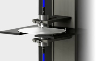
Semiconductor Wafer Thickness, Bow, Warp And Ttv Surface Description Thickness Measurement ASTM F657: The distance through a wafer between corresponding points on the front and back surface. Thickness is expressed in microns or mils (thousandths of an inch). Total Thickness Variation (TTV) ASTM F657: The difference between the maximum and minimum values of thickness encountered during a scan pattern or series of point measurements. TTV is expressed in microns or mils (thousandths of an inch). Figure above shows a wafer placed between two non-contact measurement probes. By monitoring changes between the upper probe face [...]

Tape Cartridge Movement
Tape Cartridge Movement Semiconductor Tape Cartridge Movement Positioning Description Researchers are presently working on drives with track widths in the 5 to 1 micron region. For these small widths, tape wander, properly called Lateral Tape Movement (LTM), must be less than 1 micron. This is because the track following head always lags the moving target and produces a position error signal. If the position error signal gets to be larger than about 1/10 the track width, the track cannot be read. However, it follows that the smaller the LTM, the [...]


Wafer QA/QC After Slicing And Polishing
Wafer QA/QC After Slicing And Polishing Semiconductor Wafer Qa/Qc After Slicing And Polishing Surface Description Introduction:When wafers are sliced up with wire saws, they are measured to make sure they are within the specified thickness, with minimal bow, warp, and TTV. After initial measurement, they are sorted and sent for polishing. Since polishing removes material and smoothes out the rough surfaces they need to be measured again to ensure they meet thickness guidelines and quality standards. Solution:MTI Instruments manufactures multiple systems to perform thickness measurements. From semi automated Proforma 300SA to manual [...]