
 Article: High-Performance Digitizers in Semiconductor Manufacturing Applications Gallery
Article: High-Performance Digitizers in Semiconductor Manufacturing Applications
Application Notes-GaGe, Articles-GaGe, Industry-Compliance Testing, Industry-Semiconductor, Industry-Semiconductor-GaGe, Knowledge Center-GaGe, News-GaGe, News-Industry, Whitepapers-GaGe
Article: High-Performance Digitizers in Semiconductor Manufacturing Applications
High-Performance Digitizers in Semiconductor Manufacturing Applications PC-based high-speed, high-resolution digitizers perform critical data acquisition functions during semiconductor fabrication, die packaging, and final chip testing. Introduction Data acquisition is a critical element of quality control and compliance testing during three stages of semiconductor manufacture. The first stage is fabrication, in which single-crystal semiconductor wafers are subject to various operations that leave them imprinted with micro-circuitry patterns. During the second stage, the wafers are diced up into individual silicon “die” that are packaged into final chips. The third stage involves functional testing of the final chips to [...]
 Press Release: Vitrek Supports the Semiconductor Industry’s Urgent Demand for High-Performance Test Equipment Driven by the CHIPS and Science Act Gallery
Press Release: Vitrek Supports the Semiconductor Industry’s Urgent Demand for High-Performance Test Equipment Driven by the CHIPS and Science Act
Brand-GaGe, Brand-MTI, Brand-Vitrek, Brands-All, Industry-Manufacturing, Industry-Semiconductor, Industry-Semiconductor-Vitrek, New & Press Releases, News-All Brands, News-Events, News-GaGe, News-Industry, News-MTI, News-Vitrek, Press Releases-Vitrek
Press Release: Vitrek Supports the Semiconductor Industry’s Urgent Demand for High-Performance Test Equipment Driven by the CHIPS and Science Act
The $52.7 billion legislation passed in 2022 is driving the expansion of US-based semiconductor sector; Vitrek’s product portfolio includes test and data acquisition products essential for advanced R&D and semiconductor manufacturing.
 Video: GaGe Products for the Semiconductor Industry Gallery
Video: GaGe Products for the Semiconductor Industry
Brand-GaGe, Industry-Compliance Testing, Industry-Consumer Products, Industry-Electronics, Industry-Manufacturing, Industry-Measurement Applications, Industry-R&D, Industry-Semiconductor, Industry-Semiconductor-GaGe, Industry-Semiconductor-Videos, Knowledge Center-GaGe, News-GaGe, News-Products, News-Vitrek, Videos-GaGe
 Video: MTI Products for the Semiconductor Industry Gallery
Video: MTI Products for the Semiconductor Industry
Brand-MTI, Industry-Compliance Testing, Industry-Consumer Products, Industry-Electronics, Industry-Manufacturing, Industry-Measurement Applications, Industry-R&D, Industry-Semiconductor, Industry-Semiconductor-MTI, Industry-Semiconductor-Videos, Knowledge Center-MTI, News-MTI, Videos-MTI, Videos-MTI-Capacitance Sensors, Videos-MTI-Manual Semiconductor Metrology System, Videos-MTI-Semiautomated Metrology System
 MTI Instruments Whitepaper: Capacitance Guide for Industrial Applications Gallery
MTI Instruments Whitepaper: Capacitance Guide for Industrial Applications
Brand-MTI, Industry-Aerospace, Industry-Automotive, Industry-Battery, Industry-Compliance Testing, Industry-Consumer Products, Industry-Electronics, Industry-Energy, Industry-Government/Military, Industry-Industrial Processing, Industry-Lighting, Industry-Manufacturing, Industry-Measurement Applications, Industry-OEM, Industry-R&D, Industry-Semiconductor, Industry-Semiconductor-MTI, Industry-Sensors, Industry: Transportation, Knowledge Center-MTI, News-MTI, Whitepapers-MTI
MTI Instruments Whitepaper: Capacitance Guide for Industrial Applications
Capacitance Guide for Industrial Applications This guide from MTI Instruments explains what you need to know about using electrical capacitance for measurement in industrial applications, including advanced manufacturing. Basic Principles Capacitance is the ratio of the change in an electric charge to the corresponding change in its electrical potential (i.e., voltage). Capacitors, components that that have the “capacity” to store an electric charge, consist of conductive parallel plates that don’t touch or connect with each other. Instead, these metal plates are electrically-separated by air or a layer of insulating material (i.e., the dielectric). MTI’s [...]
 Whitepaper: Why Capacitance? Benefits and Applications of Digital Capacitive Sensors Gallery
Whitepaper: Why Capacitance? Benefits and Applications of Digital Capacitive Sensors
Brand-MTI, Industry-Automotive, Industry-Compliance Testing, Industry-Consumer Products, Industry-Electronics, Industry-Industrial Processing, Industry-Manufacturing, Industry-Measurement Applications, Industry-Semiconductor, Industry-Semiconductor-MTI, Industry-Sensors, Knowledge Center-MTI, News-MTI, News-Vitrek, Whitepapers-MTI
Whitepaper: Why Capacitance? Benefits and Applications of Digital Capacitive Sensors
Industry applications illustrate the versatility and benefits of today's digital capacitive sensor technology. The electrical capacitance formed between a capacitance probe and target surface varies as a function of the distance, or gap, between those two surfaces.
 Whitepaper: Semiconductor Wafer Measurement for Increased Productivity Gallery
Whitepaper: Semiconductor Wafer Measurement for Increased Productivity
Brand-GaGe, Brand-MTI, Brand-Vitrek, Brands-All, Industry-Consumer Products, Industry-Electronics, Industry-Manufacturing, Industry-OEM, Industry-Semiconductor, Industry-Semiconductor-MTI, Knowledge Center-MTI, News-Industry, News-MTI, Whitepapers-MTI
Whitepaper: Semiconductor Wafer Measurement for Increased Productivity
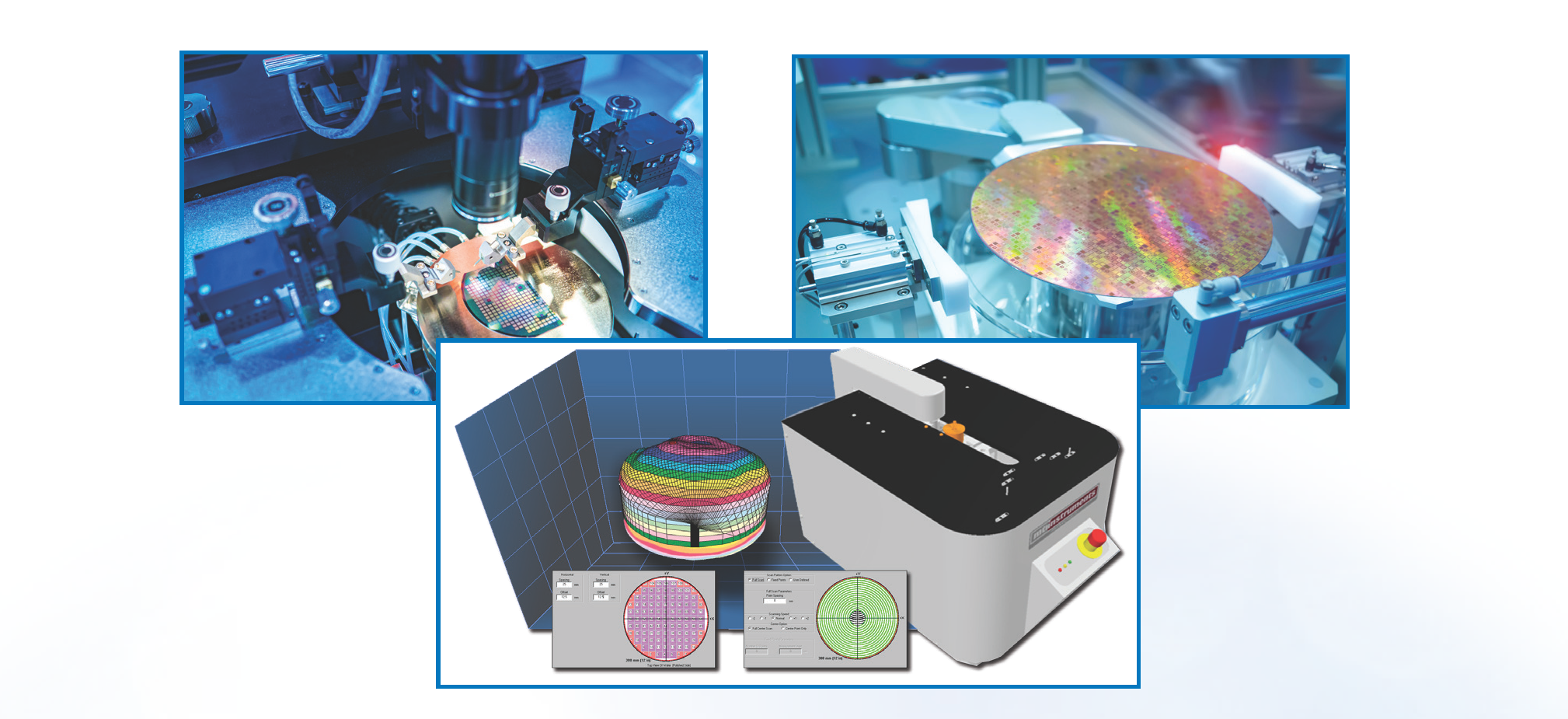
Semiconductor Wafer Measurement for Increased Productivity This three-part article describes how manufacturers leverage capacitance-based inspection systems for semiconductor wafers. The article reviews best-practices, consequences of failing to inspect semiconductor wafers and benefits of using semi-automated, fully-automated and manual systems for wafer metrology and inspection. Part 1: Why Disc Geometry Matters in Wafer Production Semiconductor wafers are cut from cylindrical silicon crystals, or ingots. The flatness of these disc-shaped wafers is controlled to tight tolerances to ensure that the entire wafer surface is suitable for integrated circuit (IC) production. If disc geometry is out-of-spec [...]
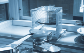
The Cost of Failing to Inspect Semiconductor Wafers
This is the second of three articles in Semiconductor Wafer Measurement for Increased Profitability. The first article in this series explains why disc geometry matters. The third article describes the benefits of using semi-automated, fully-automated, and manual systems for wafer metrology and inspection. Most semiconductor wafers are made of silicon, the second most common element in the Earth’s crust. Yet, silicon’s abundance does not mean that wafers are inexpensive. The pure form of silicon that’s used in semiconductors does not occur naturally and must be refined and mixed with a dopant that alters material properties and electrical characteristics. Silicon ingots are formed, wafers [...]
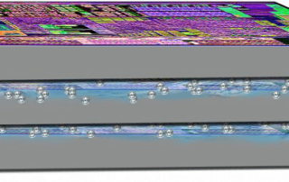
Capacitance Sensors Facilitate 3D IC Construction
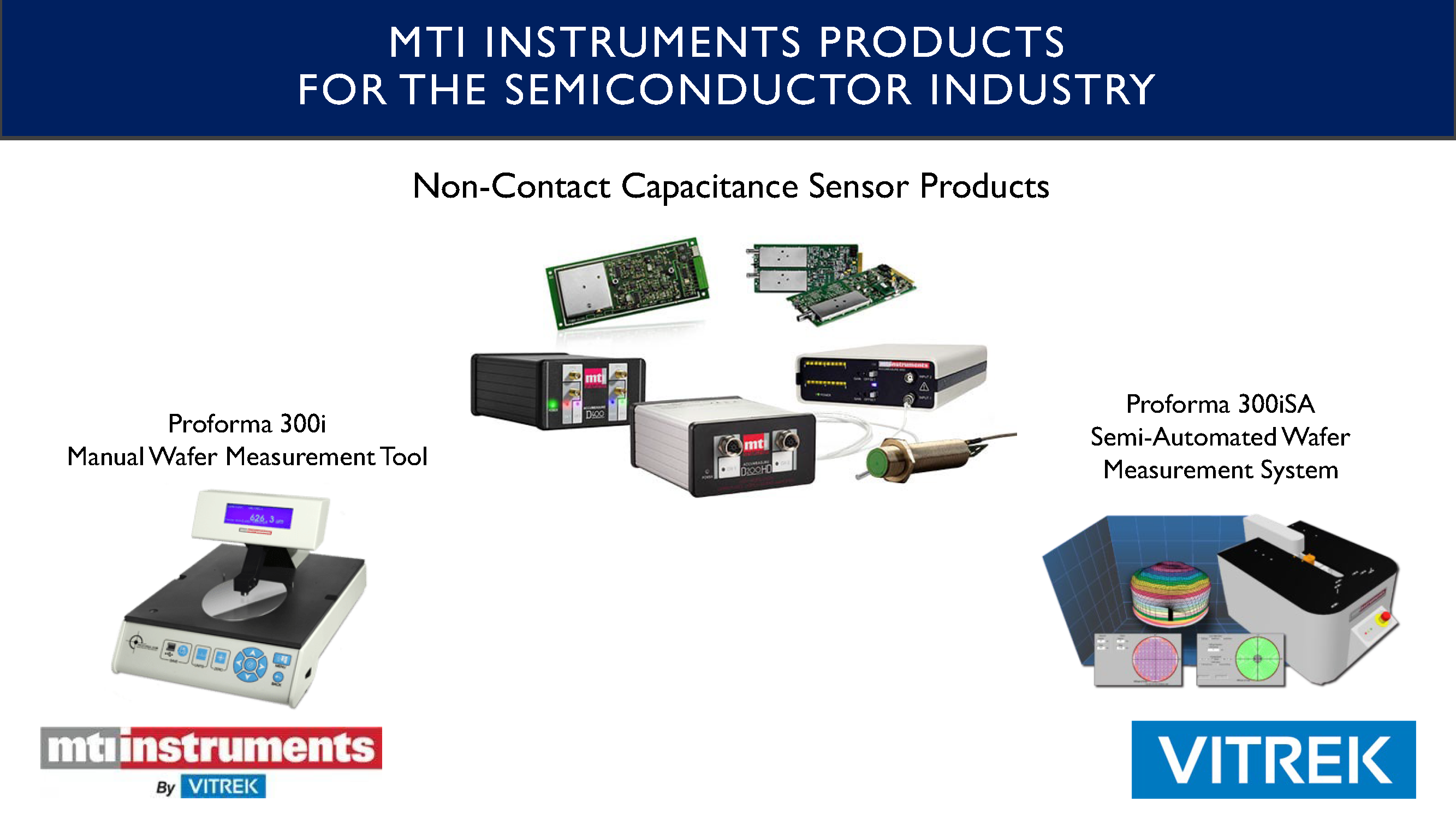
Capacitance Sensors Facilitate 3D IC Construction Semiconductor, Research & Development 3D IC Construction Distance, Positioning, Displacement Description [Application Note 70518] To boost device performance, today's semiconductor and microelectronics manufacturers are building three-dimensional integrated circuits featuring vertically-stacked silicon wafers and dies. The rationale is simple. Exploiting the Z-axis avoids the power and footprint penalties associated with two-dimensional processes. Implementing the rationale, however, is not so simple. Going vertical requires coplanar surfaces to make contact with all pins, pads, and pillars. Problem Typically, manufacturers measure the angle and gap between two planes [...]
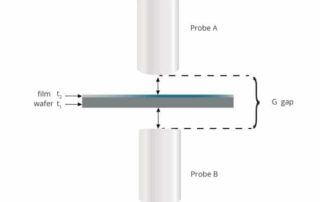




Thickness Gauge Measurement With Conductive Wafers and Thin Films
Thickness Gauge Measurement With Conductive Wafers and Thin Films Consumer Electronics Electronics Parts Profiling Thickness Description Using MTI's capacitive thickness gauge Proforma 300i with conductive wafers and thin films G = (a+b+t1+t2 ) Where G is the fixed gap between two probes When making the thickness measurement t2 can appear as t2 (film thickness) when it is a conductor, or 0 thickness when t2 is just air. So t2 will vary between the actual film thickness t2 if it's a conductor all the way down to 0 thickness if the [...]