Capacitance Sensors Track Brake Rotor Thickness Variation
[Application Note 51018] Today’s cars and trucks offer unprecedented fuel efficiencies and handling characteristics – thanks, in part, to vehicle lightweighting. Applied to all vehicle components, lightweighting lowers stress and strain to improve mileage and boost overall performance. In keeping with this trend, today’s brake rotors are thinner and lighter than those of just a few years ago. In addition, many feature cooling vents to further improve performance. These changes, however, reduce available braking surface, forcing automotive engineers to consider alternative materials and designs. Problem Because the extreme temperatures and forces generated during braking can easily lead to rotor [...]
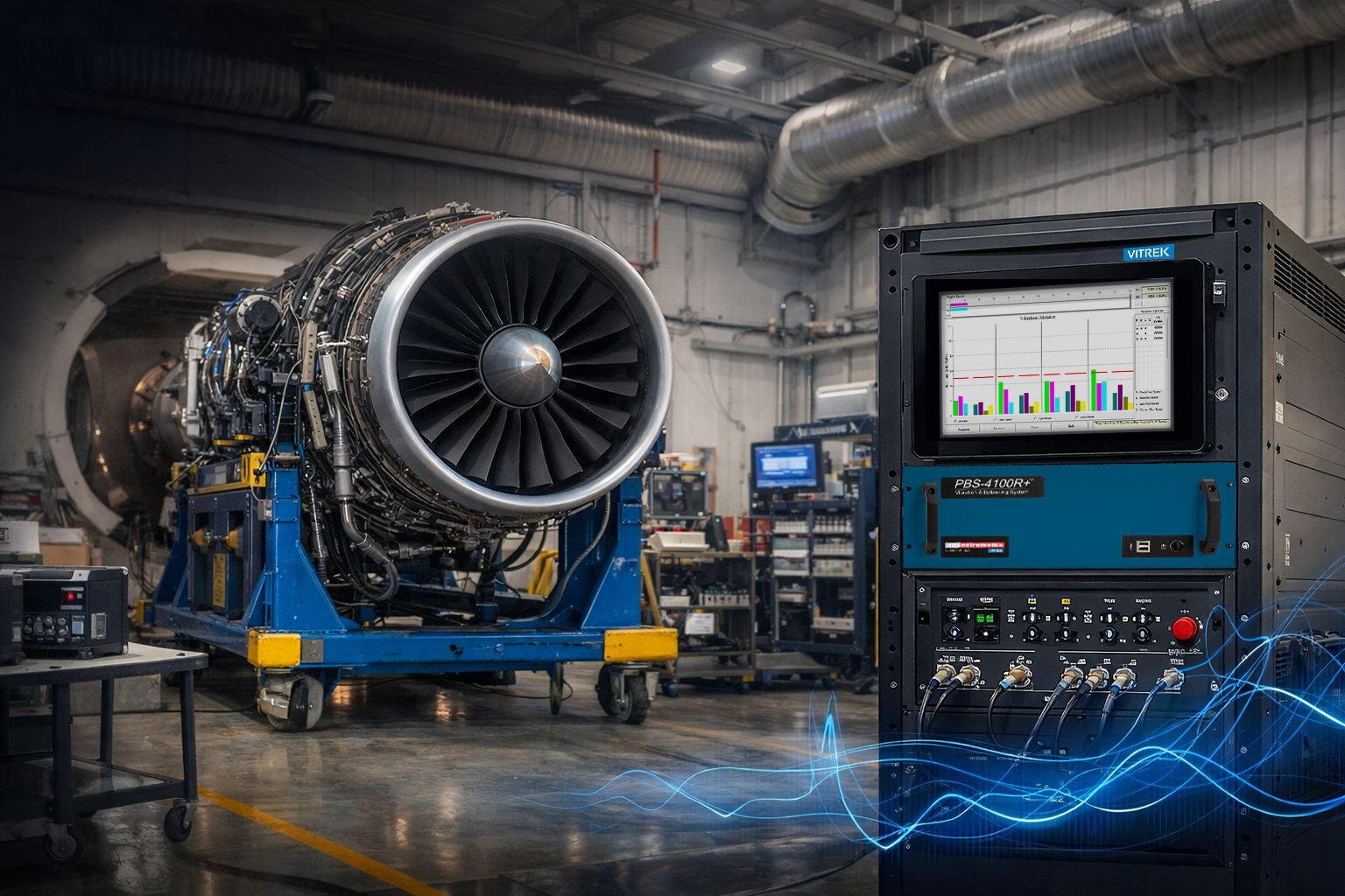
 Application Note: Replace Three Legacy Systems with One: Modernizing Aerospace/Defense Test Cells with PBS eXpress Gallery
Application Note: Replace Three Legacy Systems with One: Modernizing Aerospace/Defense Test Cells with PBS eXpress
Application Notes-MTI, Brand-MTI, Industry-Aerospace, New & Press Releases, News-Industry, News-MTI, Whitepapers-MTI
Application Note: Replace Three Legacy Systems with One: Modernizing Aerospace/Defense Test Cells with PBS eXpress
Introduction Many military/defense and commercial aerospace test cells still rely on aging analog instruments that, while functional, introduces risk through calibration challenges, legacy components, and lack of digital data access. As testing demands evolve, the industry is moving toward compact, digital platforms that simplify workflows and improve data usability. A Vitrek customer faced this challenge across multiple engine test cells. Their solution: replace two legacy systems with a single PBS eXpress R+, enabling faster setup, digital data acquisition, and automated reporting. The Challenge The customer’s test cells were built around a mix of aging instrumentation, including TrigTek tracking filters, [...]
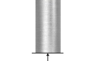
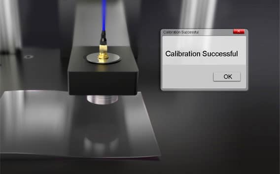
LED SUBSTRATE THICKNESS
Industry Semiconductor Applications Photolithography Using Capacitance Sensors Measurement Type Positioning Description Remember that old acronym, GIGO? Garbage in garbage out, it can apply to raw materials as well as programming. Sapphire wafers need to be of a certain quality to ensure maximum yield. Excessive TTV, Bow, and Warp lead to premature LED failure. LED manufacturers need to inspect incoming wafers. Wafer producers also need to check and control TTV, Bow and Warp. The market for sapphire wafers, driven by the growth in LED manufacturing, is booming. While the price [...]

Application Note: Why Charge Amplifiers Remain Essential in Aerospace Test Systems
Introduction Many aerospace test programs rely on charge-output piezoelectric accelerometers, force sensors, and dynamic pressure transducers because of their wide frequency response, rugged construction, and ability to capture rapidly changing events. These sensors generate extremely small electrical charge signals—often measured in picocoulombs (pC)—that are susceptible to cable capacitance effects, electrical noise, leakage currents, and environmental influences that can compromise measurement accuracy. Charge amplifiers address these challenges by converting the sensor’s high-impedance charge output into a stable, low impedance voltage signal suitable for transmission, recording, and analysis. By making measurements largely independent of cable capacitance while maintaining low noise, stable [...]
 Application Note: Accessing Digital Engine Data for Multi-Platform Aircraft Balancing with MTI PBS Systems Gallery
Application Note: Accessing Digital Engine Data for Multi-Platform Aircraft Balancing with MTI PBS Systems
Application Notes-MTI, Brand-MTI, Industry-Aerospace, New & Press Releases, News-Industry, News-MTI, Whitepapers-MTI
Application Note: Accessing Digital Engine Data for Multi-Platform Aircraft Balancing with MTI PBS Systems
Introduction Modern aircraft engines are no longer dependent solely on discrete analog sensors for critical performance data. Increasingly, vibration amplitudes, phase information, and engine speed are transmitted digitally through aircraft data buses such as ARINC 429 and ARINC 664 Part 7 (AFDX). Yet in many MRO environments, balancing systems continue to rely on accelerometers and tachometer pickups—introducing additional setup time, cabling complexity, and potential variability in measurements. This disconnect between available digital data and traditional measurement approaches creates inefficiencies, particularly for facilities servicing multiple aircraft platforms. For organizations supporting a diverse fleet, the opportunity is clear: leverage the aircraft’s [...]
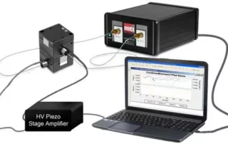
PIEZO STAGE POSITIONING
Industry Consumer Electronics Applications Piezo Stage Measurement Type Positioning Description Positioning stages using piezoelectric stack actuators (PEA) have very high resolution. However, it is difficult to achieve precise dynamic motion tracking using traditional linear controllers such as PID due to the inherent hysteresis nonlinearity of piezoelectric materials and the phase lag associated with such controllers. Capacitance Sensors are ideal for measuring the actual piezo stage position and correcting for the inherent nonlinearity through closed loop feedback. They have the stability, bandwidth and high resolution needed to do the job. [...]

WAFER QA/QC AFTER SLICING AND POLISHING
Industry Semiconductor Applications Wafer Qa/Qc After Slicing And Polishing Measurement Type Surface Description When wafers are sliced up with wire saws, they are measured to make sure they are within the specified thickness, with minimal bow, warp, and TTV. After initial measurement, they are sorted and sent for polishing. Since polishing removes material and smoothes out the rough surfaces they need to be measured again to ensure they meet thickness guidelines and quality standards. Solution: MTI Instruments manufactures multiple systems to perform thickness measurements. From semi automated Proforma 300SA to manual wafer [...]
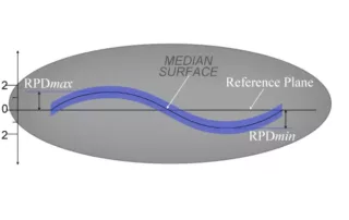
ABOUT WAFER BOW AND WARP MEASUREMENT SYSTEMS
Thickness Measurement for Metrology Systems ASTM F657: The distance through a wafer between corresponding points on the front and back surface. Thickness is expressed in microns or mils (thousandths of an inch). Total Thickness Variation (TTV) ASTM F657: The difference between the maximum and minimum values of thickness encountered during a scan pattern or series of point measurements. TTV is expressed in microns or mils (thousandths of an inch). ASTM F534 3.1.2: The deviation of the center point of the median surface of a free, unclamped wafer from the median [...]

LITHOGRAPHY OPTICS POSITION FOCUS
Industry Semiconductor Applications Photolithography Using Capacitance Sensors Measurement Type Positioning Description One specific area where capacitance systems excel is high resolution focusing of complex lens systems such as those found in atomic force microscopes, vision inspection machines and photolithography tools. In a multi-million dollar photolithography tool, high accuracy, nanometer resolution and maximum thermal stability are absolutely critical to maintain proper focus and obtain integrated circuit line widths as small as 45 nanometers. Additionally, most systems demand low power consumption and maximum heat dissipation to eliminate any adverse affects from [...]

GAAS SUBSTRATE THICKNESS MEASUREMENT
Industry Semiconductor Applications Gaas Substrate Thickness Measurement Measurement Type Thickness Description Measuring Thickness of Wafers with Different Chemistries Introduction: Silicon wafers are ordinarily highly conductive and easy to measure with standard capacitive displacement sensors (See MTI’s Proforma 300i). Measuring the thickness of GaAs wafers that have high bulk resistivity (>10k Ohm/cm) is a little more difficult because the wafers act as non-conductive insulators in a capacitive sensor’s measuring field. Fortunately, MTI has a solution to this problem. Solution: It’s possible to measure the thickness and TTV of high resistivity semiconducting wafers (like GaAs) using non-contact capacitive [...]