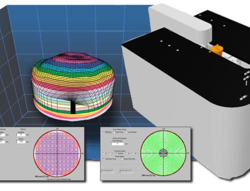
Thickness and TTV of Semiconducting Wafers
Description
Introduction: 
Solution: 
- The measurement is non contact so is ideal for surfaces that shouldn’t be touched
- Highly accurate thickness measurements typically less than a micron (.00004 inch) can be performed
- A special dielectric mode of operation for semi-conducting wafer measurement provides highly accurate thickness measurements
- User adjustable digital filtering/smoothing is selectable and a 20,000 samples/second rate will meet almost all process measurement applications
- Easily calibrated to measure thickness of insulating material, without knowing the dielectric constant of the materials being measured, if you have a sample of known thicknesses
- Directly reads the thickness and sends the results to a standard PC running MTI’s Digital Accumeasure TM display program
The same program assists in setting up the initial calibration needed to measure thickness with a few simple steps that are easy to follow.
 |
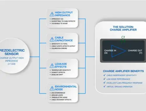
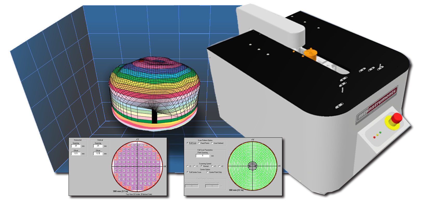
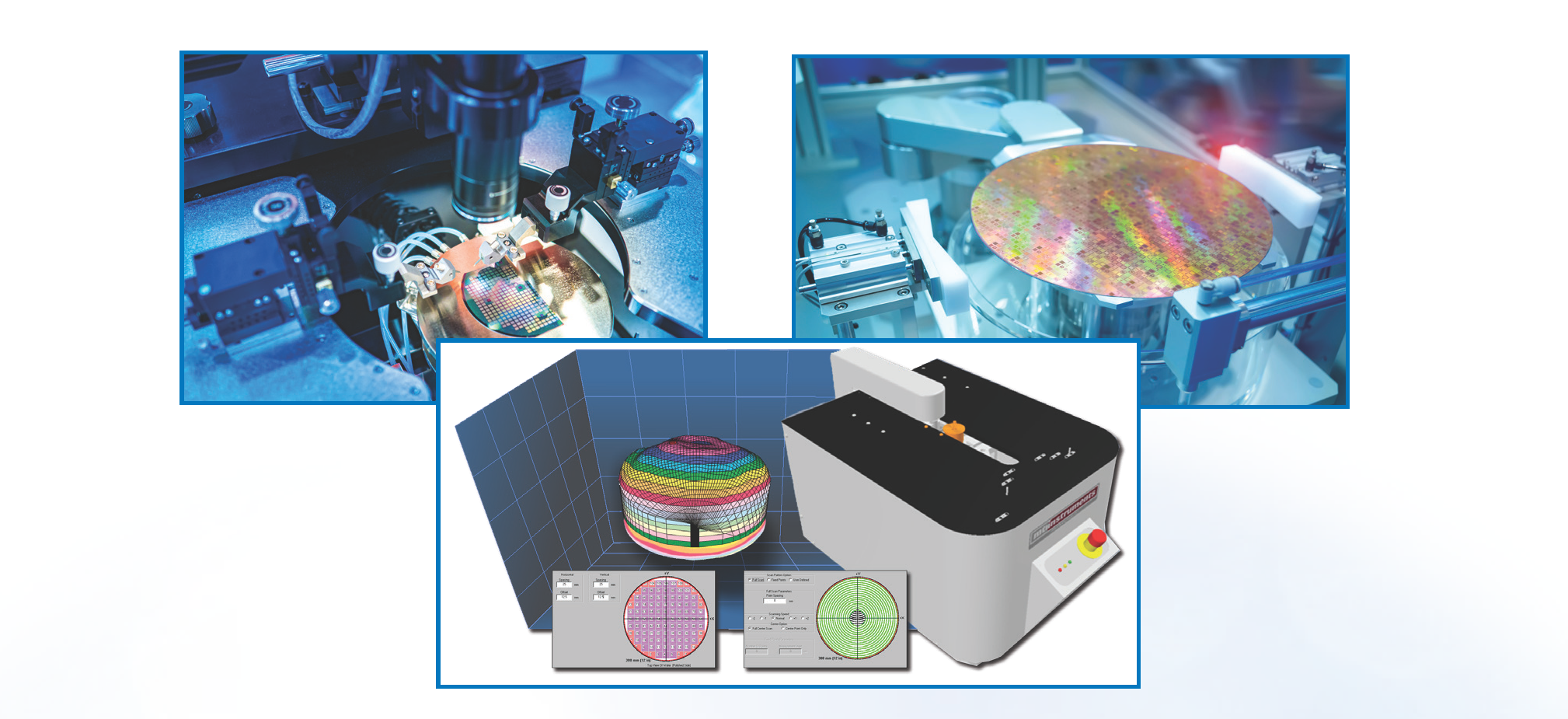
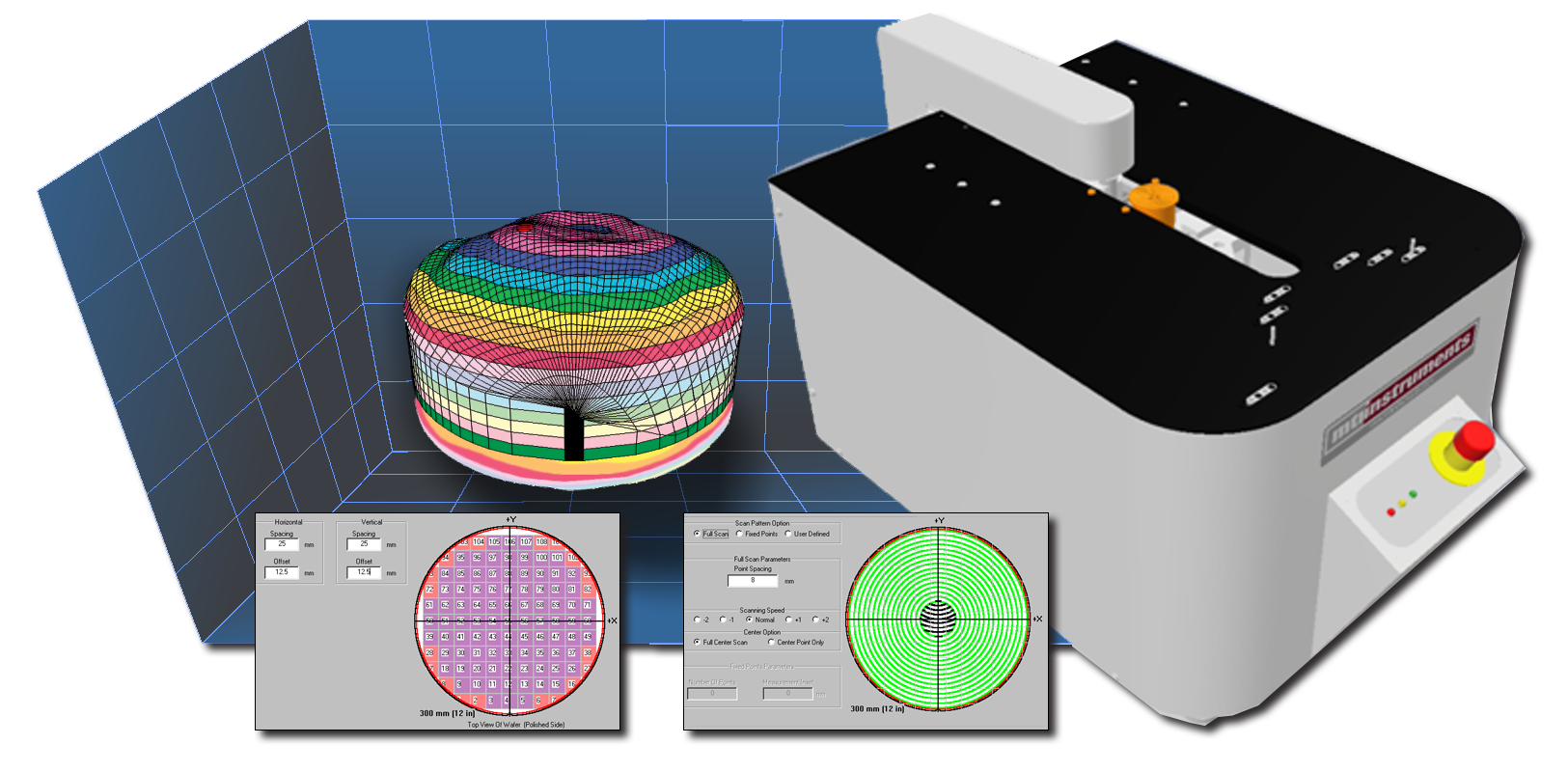
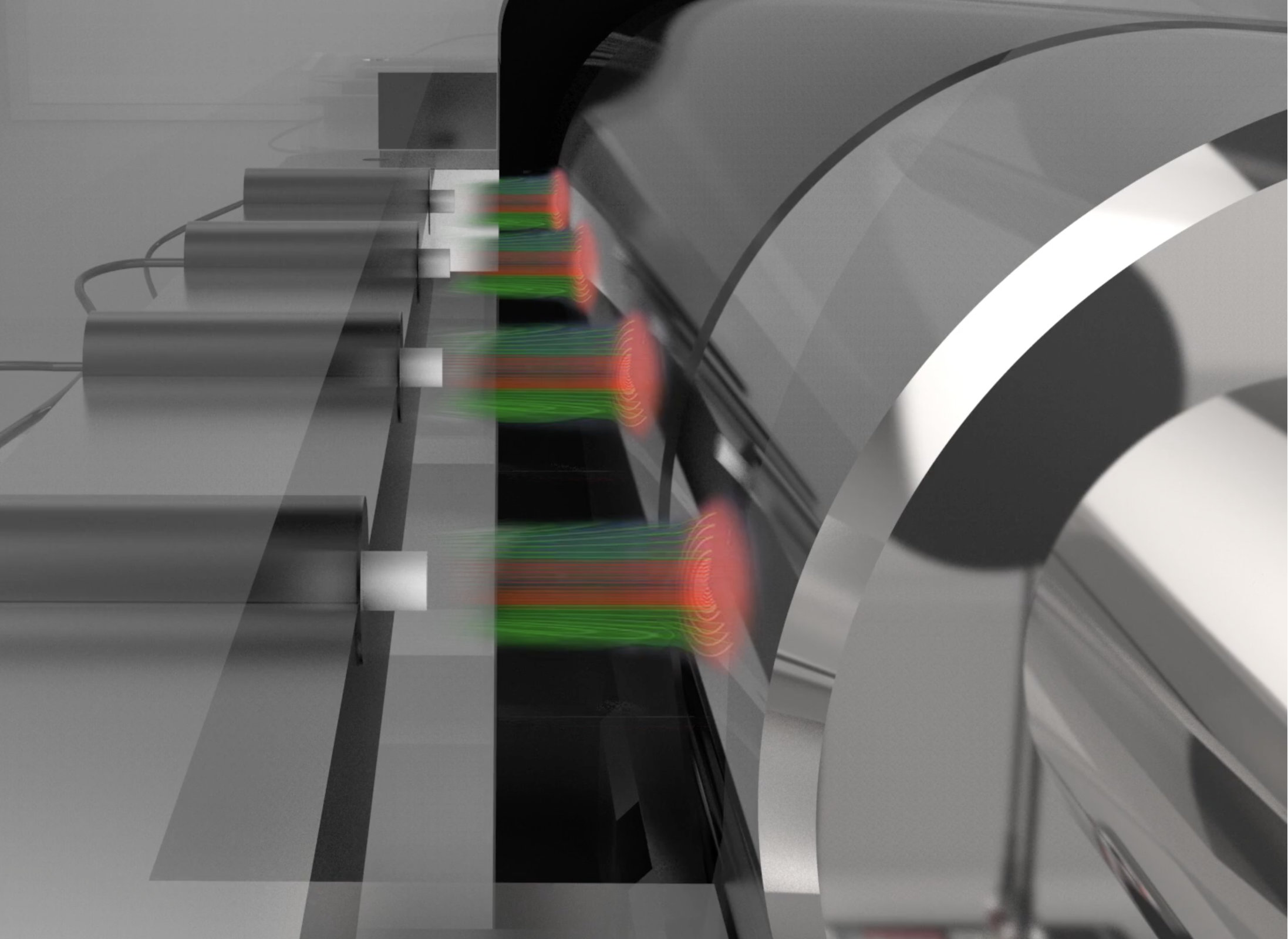
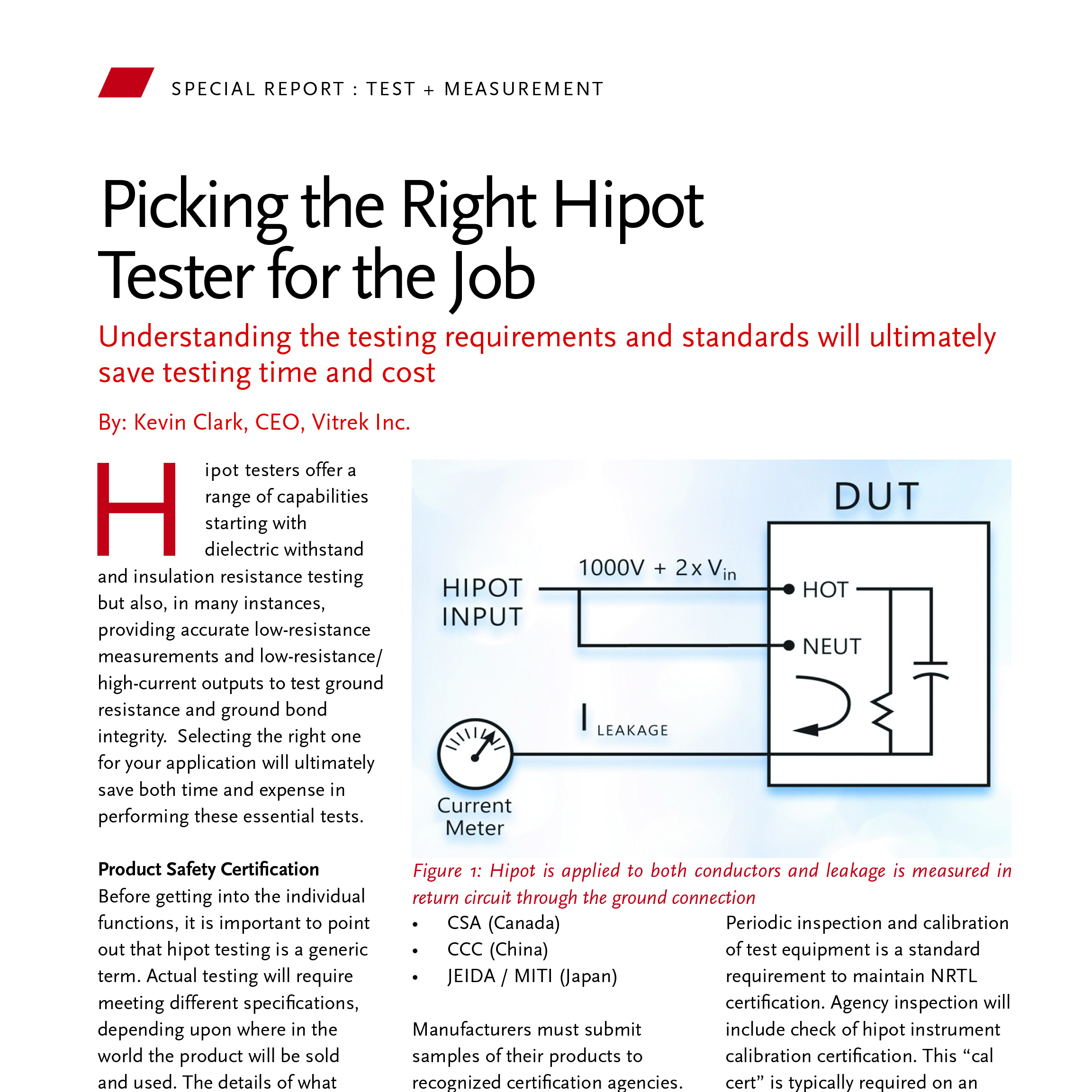
Placing a GaAs wafer between a capacitance probe and a ground plane creates a capacitive circuit that can be analyzed to determine total thickness |
Set up is quick and easy.
Simply determine the range limit of the probe (by adjusting the height until the indicator on the amplifier just turns blue and before it turns red) and entering zero in the first sample thickness. Press “calibrate” and place a wafer of known thickness between the probe and ground plane. Now enter the known thickness into the second sample thickness and calibrate the second sample. This has stored the dielectric constant which will be used to measure all remaining wafers. Digital Accumeasure TM Capacitance Amplifier is also perfect for measuring other non-conductive commodities such as Plastic, Glass, Optical Disc’s, Paper, and Rubber.
MTI Instruments, Inc. offers several styles and types of non-contact sensors that can be customized to your exact requirements. If you have a difficult application to solve, contact our experienced team of application engineers who will thoroughly analyze your requirements and guide you to a practical, cost-effective solution.


