
Laser Measurement & Characterization of Flat Panel Displays
Laser Measurement & Characterization of Flat Panel Displays Customer Case This customer's application involves the characterization of flat panel displays (used in laptop computers, computer game displays, etc.) via laser scanning. The laser is bounced off a number of mirrors and then through lenses, from which it is scattered. The scattered laser light must then be analyzed in order to determine the quality of the flat panel display. This laser measurement system is used not only by flat panel display industries, but also by disk drive manufacturers to analyze platter quality and, in the near future, for characterizing silicon [...]
 Advantages of Measuring Semiconductor Thin Film Thickness with Capacitance Gallery
Advantages of Measuring Semiconductor Thin Film Thickness with Capacitance
Application Notes-MTI, Brand-MTI, Industry-Compliance Testing, Industry-Electronics, Industry-Manufacturing, Industry-R&D, Industry-Semiconductor, Industry-Semiconductor-MTI, Industry-Sensors, Products-MTI-Capacitance, Products-MTI-Laser/Fiber Optic, Products-MTI-Semiconductor/Metrology, Z-REPUB, z1
Advantages of Measuring Semiconductor Thin Film Thickness with Capacitance
Thin Film Thickness Measurement Using Capacitance in the Semiconductor Industry In the semiconductor industry, the precise measurement of thin film thickness is crucial for ensuring the quality and functionality of wafer coatings. Thin films are deposited onto silicon and other wafer materials one atomic layer at a time, and the thickness of these coatings significantly impacts the wafer’s electrical, optical, and mechanical properties. Thin film thickness measurement is particularly important for semiconductor wafers, which may have either conductive metallic films or non-conductive metal oxide films deposited onto them. Common deposition methods include chemical vapor deposition (CVD) and physical vapor [...]
Laser Signals Striking Silicon-Diode Target
Laser Signals Striking Silicon-Diode Target Customer Case The customer wants to capture the output of some silicon diodes looking at a laser target. The typical signal is anywhere from 20mv to 1V in amplitude and 0 to 15ns in length. There are up to 16 of these diodes that are looking at the same target. Each diode has a different filter so the post-trigger depth and amplitude-scale must be user-adjustable. Their main interest is to sample and digitize the signals for archiving, with later retrieval and plotting. Fancy software is not needed for display as the data is gathered [...]
Optical Scanning of Drive Media
Optical Scanning of Drive Media Customer Case The customer's application is optical scanning for drive testing. The goal is to identify burnt or damaged spots on the disk. The scanning system is generally used in Quality Control, Head-Disk Interaction and Failure Analysis. There is a need for continuous acquisition during the spiral scan. The speed of the disk is 10,000 RPM and the requirement is to capture 65,000 to 80,000 samples each revolution. A single channel is needed for the acquisition at 10 MegaSamples/second or greater. High vertical resolution will aid in measuring the properties and ultimately the degradation [...]
Disk Drive Track Scanning
Disk Drive Track Scanning Customer Case The customer is trying to digitize an 83 millisecond long signal coming out of a disk mounted on a rotary motor. This corresponds to one full revolution of the disk. The analog signal coming out of the Device Under Test (DUT) is of approximately 2 MHz bandwidth. Currently, the customer is sampling at 10 MSPS and would like to increase the oversampling to get better time resolution. At present, they are using a CompuScope 225 - 1M, which has sufficient memory to digitize the entire revolution in on-board memory at the 10 MSPS [...]
How Often Should Vibration Analysis Be Performed?
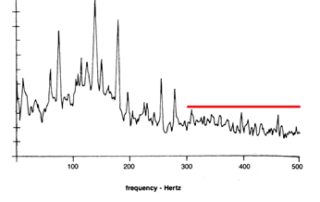
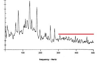
How Often Should Vibration Analysis Be Performed? Once a customer takes delivery of a PBS system and learns how to use it, the next logical question is: “How often should we use it?” At a minimum, your approved maintenance program (whether it’s a program developed by your operation, or the maintenance procedures outlined by the engine/airframe manufacturer) will tell you about the intervals at which to perform a vibration analysis. Usually, there is a procedure to specify how an engine vibration analysis and balance need be only completed when squawked by a pilot or after the completion of maintenance [...]
MEMS-Based High Throughput Screening
MEMS-Based High Throughput Screening Customer Case The customer needs to do frequency analysis to determine the resonant frequency of an oscillating micro-fabricated device. They will use a Laser Doppler Vibrometer to monitor the physical oscillation. This is an instrument that looks at the light reflected from the surface of a moving part to determine the velocity or relative position of the part. Analysis of the motion as a function of the driving frequency determines the resonant frequency. Upon excitation at the resonant frequency, the motion is at its maximum. The expected resonant frequencies are on the order of 1 [...]
Automatic Accelerometer Calibration System
Automatic Accelerometer Calibration System Customer Case The customer's Automated Accelerometer Calibration System provides NIST traceable calibration of most accelerometer types, whether self-generating piezo-electric or accelerometers requiring current or voltage excitation. The output of the accelerometer can be charge or voltage, single- ended or differential, AC or DC coupled, isolated or grounded. In building the automatic calibration system, the need is for optimum versatility with regards to the data acquisition card. LabVIEW is the desired control software, and Signal to Noise Ratio and high vertical resolution is of utmost importance for the small variations that occur in Vibration and Shock [...]
 Contact vs. Non-Contact Measurement and Linear Displacement Sensors Gallery
Contact vs. Non-Contact Measurement and Linear Displacement Sensors
Application Notes-MTI, Brand-MTI, Industry-Compliance Testing, Industry-Consumer Products, Industry-Electronics, Industry-Manufacturing, Industry-Semiconductor, Industry-Semiconductor-MTI, Industry-Sensors, Products-MTI-Capacitance, Z-REPUB, z1, ZOK
Contact vs. Non-Contact Measurement and Linear Displacement Sensors
Contact vs. Non-Contact Measurements Choosing between a contact measurement system and a non-contact measurement system requires careful evaluation of your application’s performance needs, material properties, environmental conditions, and measurement goals. Each system type offers unique advantages- and understanding these distinctions can help you make a more informed decision. Let's explores how contact and non-contact measurement techniques work, their strengths and limitations, and where they’re best applied. What Are Contact Measurement Systems? Contact measurement systems involve tools and sensors that physically touch the object to determine various physical characteristics. These systems are widely used in dimensional metrology, offering high precision, [...]


Capacitance Sensors vs. Eddy Current Sensors Application Note
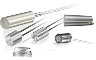
Capacitance Sensors vs. Eddy Current Sensors Application Note Capacitance sensors and Eddy current sensors are both used for non-contact measurements. Capacitive probes use electric fields to measure the distance from the sensor face to the surface of a target that is typically conductive and grounded. Eddy current probes use an alternating AC current to induce a magnetic field in a conductive target instead. In turn, the induced magnetic field produces a back magnetic field that is proportional to the gap between the probe face and the target. In a recent application note, MTI Instruments examines the differences between capacitance [...]