

Thermal Expansion On Automobile Engine
Thermal Expansion On Automobile Engine Automotive Thermal Expansion On Automobile Engine Dimensions Description For years the sole purpose of the oil pan was to act as a reservoir for the engine lubricant. Some modern engines now utilize the pan as a structural component. It is machined from a rigid steel or aluminum casting and designed to support the lower portion of the crankshaft bearings and rear main seal. This development has introduced a potential problem area that must be analyzed. As engines go through heating and cooling cycles it is [...]

Robotic Weld Inspection
Automotive Robotic Weld Inspection Presence/Absence Description

Sheet Metal Monitoring
Sheet Metal Monitoring Automotive Sheet Metal Monitoring Thickness Description Introduction: When sheet metal is formed in a continuous process it needs monitoring during the actual feed prior to machining or forming to prevent defects and scrap.  One way to accomplish this is to use a laser sensor to measure the thickness. Problem: A major electrical equipment manufacturer needed a way to monitor the incoming material just prior to shearing and forming. The device needed to be robust, non-contact, reliable, accurate, and fast. The client would be using their data acquisition [...]

Wire Bonding
Wire Bonding Semiconductor Wire Bonding Level Description Introduction What is Wire Bonding? Wire bonding is a critical semiconductor manufacturing process that creates electrical connections between integrated circuits (ICs) and their packaging substrates. This wire bonding technique uses ultra-thin bond wires, typically made of gold or aluminum, to establish reliable electrical pathways in microelectronics applications. Understanding Wire Bond Fundamentals A typical wire bond consists of bonded wire connecting a die pad to a substrate pad on a PC board. The bond wire diameter varies between 18 and 50 microns, with 25 microns [...]

GaAs Substrate Thickness Measurement
Semiconductor Gaas Substrate Thickness Measurement Thickness Description Measuring Thickness of Wafers with Different Chemistries Introduction:  Silicon wafers are ordinarily highly conductive and easy to measure with standard capacitive displacement sensors (See MTI's Proforma 300i). Measuring the thickness of GaAs wafers that have high bulk resistivity (>10k Ohm/cm) is a little more difficult because the wafers act as non-conductive insulators in a capacitive sensor's measuring field. Fortunately, MTI has a solution to this problem. Solution:  It’s possible to measure the thickness and TTV of high resistivity semiconducting wafers (like GaAs) using non-contact [...]

Photolithography Using Capacitance Sensors
Photolithography Using Capacitance Sensors Semiconductor Photolithography Using Capacitance Sensors Positioning Description When it comes to photolithography, how accurate are our sensors? Accurate enough to measure this: ​   Photo by D. Carr and H. Craighead, Cornell The world's smallest guitar is 10 micrometers long -- about the size of a single cell -- with six strings each about 50 nanometers, or 100 atoms, wide. Made by Cornell University researchers from crystalline silicon, it demonstrates a new technology for a new generation of electromechanical devices. Even the world’s smallest guitar’s 2 micron [...]
THICKNESS INFORMATION OF COMPOSITE MATERIALS
Composite materials consist of two or more materials which include a substrate or base material such as paper, cotton cloth, or glass cloth along with a resin or adhesive such as epoxy, melamine, or silicone. To make a thermoset laminate, the base material is coated with the adhesive so that layers of material can be pressed under heat and pressure into sheet form. The Problem: Composite material thickness needed to be verified prior to forming or machining. Due to the size of the sheets typical measurement techniques were not suitable. A consistent method to accurately measure the board thickness [...]

Hard Drive Position
Semiconductor Hard Drive Position Positioning Description

LED Substrate Thickness
LED Substrate Thickness Semiconductor Led Substrate Thickness Thickness Description Remember that old acronym, GIGO?  Garbage in garbage out, it can apply to raw materials as well as programming. Sapphire wafers need to be of a certain quality to ensure maximum yield. Excessive TTV, Bow, and Warp lead to premature LED failure. LED manufacturers need to inspect incoming wafers. Wafer producers also need to check and control TTV, Bow and Warp. The market for sapphire wafers, driven by the growth in LED manufacturing, is booming. While the price has come down [...]
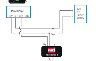

Adding a Digital Panel Meter to MTI Analog Output Products
Adding a Digital Panel Meter to MTI Analog Output Products Consumer Electronics Electronics Parts Profiling Thickness Description Some MTI Products with Analog outputs, Accumeasure 9000 and Microtrak 3 laser How To Use Digital Displays with Analog Outputs MTI Microtrak 3 Lasers and some of our Accumeasure amplifiers such as the Accumeasure 9000 only have analog outputs. If you wish to add a digital display, then the Lascar Panel pilot © makes a nice cost effective (~ $110) addition - Fig 1. These Digital panel meters have both 1 [...]