
 Whitepaper: Why Capacitance? Benefits and Applications of Digital Capacitive Sensors Gallery
Whitepaper: Why Capacitance? Benefits and Applications of Digital Capacitive Sensors
Brand-MTI, Industry-Automotive, Industry-Compliance Testing, Industry-Consumer Products, Industry-Electronics, Industry-Industrial Processing, Industry-Manufacturing, Industry-Measurement Applications, Industry-Semiconductor, Industry-Semiconductor-MTI, Industry-Sensors, Knowledge Center-MTI, News-MTI, News-Vitrek, Whitepapers-MTI
Whitepaper: Why Capacitance? Benefits and Applications of Digital Capacitive Sensors
Industry applications illustrate the versatility and benefits of today's digital capacitive sensor technology. The electrical capacitance formed between a capacitance probe and target surface varies as a function of the distance, or gap, between those two surfaces.
 Whitepaper: Semiconductor Wafer Measurement for Increased Productivity Gallery
Whitepaper: Semiconductor Wafer Measurement for Increased Productivity
Brand-GaGe, Brand-MTI, Brand-Vitrek, Brands-All, Industry-Consumer Products, Industry-Electronics, Industry-Manufacturing, Industry-OEM, Industry-Semiconductor, Industry-Semiconductor-MTI, Knowledge Center-MTI, News-Industry, News-MTI, Whitepapers-MTI
Whitepaper: Semiconductor Wafer Measurement for Increased Productivity
Semiconductor Wafer Measurement for Increased Productivity This three-part article describes how manufacturers leverage capacitance-based inspection systems for semiconductor wafers. The article reviews best-practices, consequences of failing to inspect semiconductor wafers and benefits of using semi-automated, fully-automated and manual systems for wafer metrology and inspection. Part 1: Why Disc Geometry Matters in Wafer Production Semiconductor wafers are cut from cylindrical silicon crystals, or ingots. The flatness of these disc-shaped wafers is controlled to tight tolerances to ensure that the entire wafer surface is suitable for integrated circuit (IC) production. If disc geometry is out-of-spec [...]
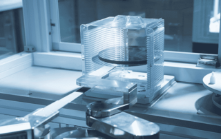
The Cost of Failing to Inspect Semiconductor Wafers
This is the second of three articles in Semiconductor Wafer Measurement for Increased Profitability. The first article in this series explains why disc geometry matters. The third article describes the benefits of using semi-automated, fully-automated, and manual systems for wafer metrology and inspection. Most semiconductor wafers are made of silicon, the second most common element in the Earth’s crust. Yet, silicon’s abundance does not mean that wafers are inexpensive. The pure form of silicon that’s used in semiconductors does not occur naturally and must be refined and mixed with a dopant that alters material properties and electrical characteristics. Silicon ingots are formed, wafers [...]
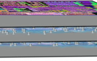
Capacitance Sensors Facilitate 3D IC Construction
Capacitance Sensors Facilitate 3D IC Construction Semiconductor, Research & Development 3D IC Construction Distance, Positioning, Displacement Description [Application Note 70518] To boost device performance, today's semiconductor and microelectronics manufacturers are building three-dimensional integrated circuits featuring vertically-stacked silicon wafers and dies. The rationale is simple. Exploiting the Z-axis avoids the power and footprint penalties associated with two-dimensional processes. Implementing the rationale, however, is not so simple. Going vertical requires coplanar surfaces to make contact with all pins, pads, and pillars. Problem Typically, manufacturers measure the angle and gap between two planes [...]
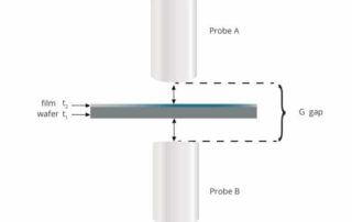
Thickness Gauge Measurement With Conductive Wafers and Thin Films
Thickness Gauge Measurement With Conductive Wafers and Thin Films Consumer Electronics Electronics Parts Profiling Thickness Description Using MTI's capacitive thickness gauge Proforma 300i with conductive wafers and thin films G = (a+b+t1+t2 ) Where G is the fixed gap between two probes When making the thickness measurement t2 can appear as t2 (film thickness) when it is a conductor, or 0 thickness when t2 is just air. So t2 will vary between the actual film thickness t2 if it's a conductor all the way down to 0 thickness if the [...]

Semiconductor Wafer Lapping and Displacement Measurement
Introduction This application note explains how MTI's Accumeasure technology was used with a lapping machine to measure displacement (wafer material removal) and determine the new semiconductor wafer thickness. Changes in electrical capacitance (displacement) were measured and then directly converted into a 24-bit digital reading to obtain precise digital thickness measurements. During lapping, a wafer of known start thickness is placed on a rotary lapping table. The backside of the wafer faces downward and toward a lapping surface that rotates and removes unwanted material. The amount of material that is removed varies by device type, and the entire semiconductor [...]
 MTI’s Accumeasure HD Amplifier vs. SmarAct’s PicoScale Interferometer Gallery
MTI’s Accumeasure HD Amplifier vs. SmarAct’s PicoScale Interferometer
App Notes, Application Notes-MTI, Applications, Brand-MTI, Brands, Editorials, Industry, Industry-R&D, Industry-Semiconductor, Industry-Semiconductor-MTI, Z-REPUB, z1
MTI’s Accumeasure HD Amplifier vs. SmarAct’s PicoScale Interferometer
MTI's Accumeasure HD Amplifier vs. SmarAct's PicoScale Interferometer Research & Development Piezoceramic, 1-3 Pzt / Polymer Composite And Pvdf Film Amplitude Description This application note compares MTI's Accumeasure HD amplifier to SmarAct's Picoscale interferometer in terms of resolution and accuracy for very small displacement measurements. Specifically, this comparison focuses on minimum expected resolution and the effects of noise on accuracy. High resolution interferometers are widely regarded as the instrument of choice for the type of measurements described in this application note, but MTI's technology provides exceptional accuracy and stability. Moreover, the [...]

Connecting Encoders to MTI’s Digital Accumeasure
Connecting Encoders to MTI's Digital Accumeasure MTI's Digital Accumeasure D has the ability to accept one or two digital quadrature encoders. The encoders can be linear slide-type or rotary. Digital encoders allow for tracking the position of capacitive probes such that you can synchronize a probe's position with the probe's displacement data. Two common examples are: Rotary shaft runout: shaft (radial) displacement vs. angular encoder position X/Y position of probes measuring wafer thickness (map wafer thickness) Accumeasure software (basic and measurement) allows the display of instantaneous encoder counts as well as probe displacement data; however, [...]
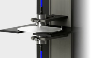
Thickness and TTV of Semiconducting Wafers
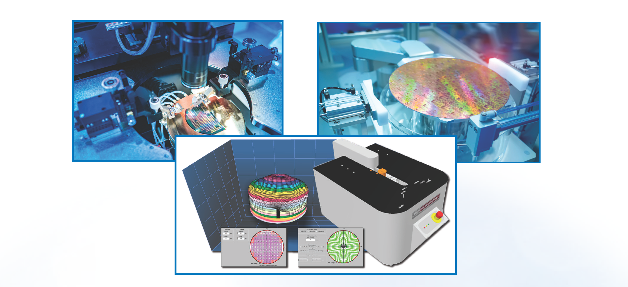
Thickness and TTV of Semiconducting Wafers Semiconductor Thickness And TTV Of Semiconducting Wafers Thickness Description Introduction:  Silicon wafers are ordinarily highly conductive and easy to measure with standard capacitive displacement sensors (See MTI’s Proforma 300i). Measuring the thickness of GaAs wafers that have high bulk resistivity (>10k Ohm/cm) is a little more difficult because the wafers act as non-conductive insulators in a capacitive sensors measuring field. Fortunately, MTI has a solution to this problem. Solution:  It’s possible to measure the thickness and TTV of high resistivity semiconducting wafers (like GaAs) [...]



Lithography Optics Position Focus
Lithography Optics Position Focus Semiconductor Lithography Optics Position Focus Positioning Description One specific area where capacitance systems excel is high resolution focusing of complex lens systems such as those found in atomic force microscopes, vision inspection machines and photolithography tools. In a multi-million dollar photolithography tool, high accuracy, nanometer resolution and maximum thermal stability are absolutely critical to maintain proper focus and obtain integrated circuit line widths as small as 45 nanometers. Additionally, most systems demand low power consumption and maximum heat dissipation to eliminate any adverse affects from temperature [...]