Introduction
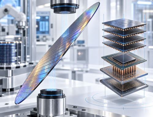
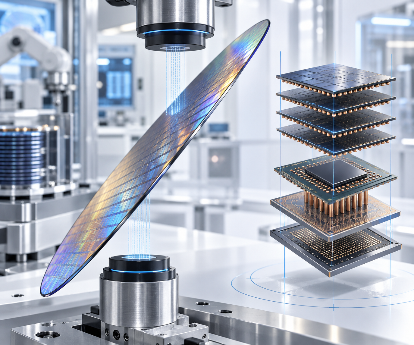
AI accelerators, high-performance computing systems, high bandwidth memory and chiplet-based devices increasingly rely on 2.5D and 3D advanced packaging processes that combine logic, memory, interposers and specialized dies within tightly controlled structures.
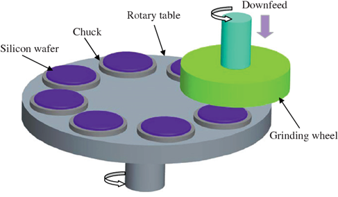
Before stacking or bonding, wafers may undergo coarse grinding, fine grinding, polishing and other backside processes. These operations must remove substantial material while maintaining the thickness and geometry required by the package design.
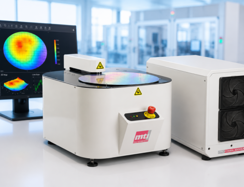
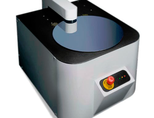
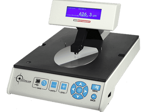
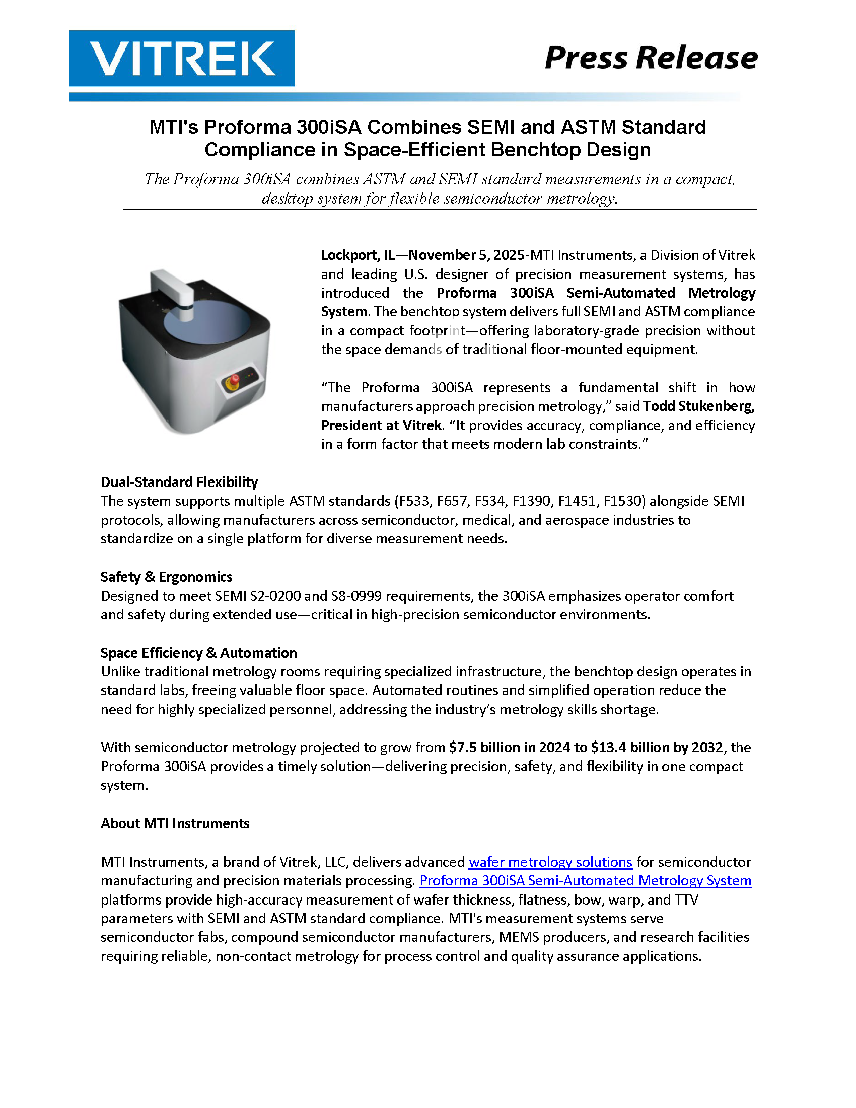
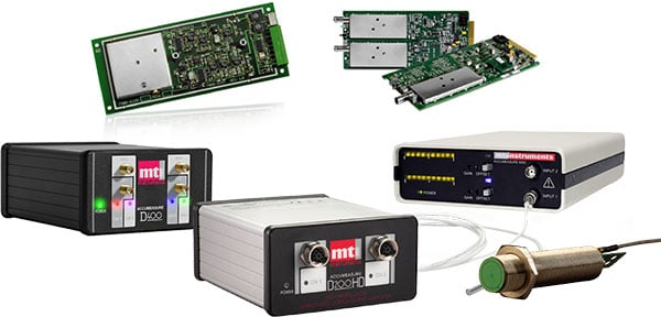
This application note explains how the MTI Instruments Proforma 300i and Proforma 300iSA can be used at defined process checkpoints to verify wafer thickness, evaluate uniformity and identify process changes before wafers proceed to costly downstream packaging operations.
The Measurement Challenge
As substrate thickness decreases, the wafer also loses mechanical stiffness. Thin wafers are more vulnerable to deflection, handling damage, breakage, bow and warp.
Backside processing must control wafer thickness at both intermediate and final stages. It must also maintain total thickness variation and uniformity across the wafer within the required limits.
As material is removed, manufacturers must monitor bow and warp and ensure that results remain repeatable from wafer to wafer and lot to lot. A single center-point measurement may confirm nominal thickness while missing localized variation elsewhere on the wafer. Contact-based measurement can also introduce force that deflects a thin substrate or risks damage to a sensitive surface.
Manufacturers need a repeatable, non-contact method that can be incorporated between process steps without creating a significant inspection bottleneck.
The Measurement Approach
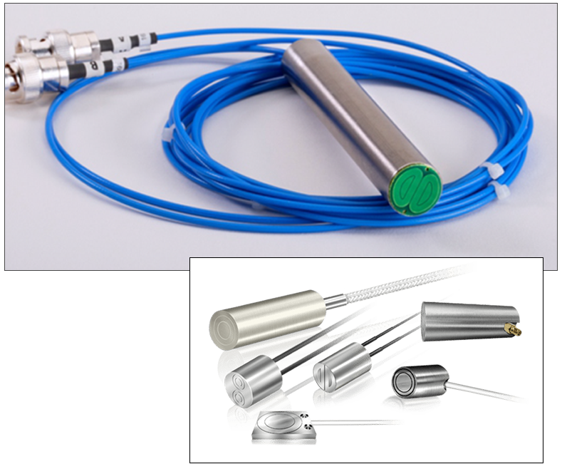
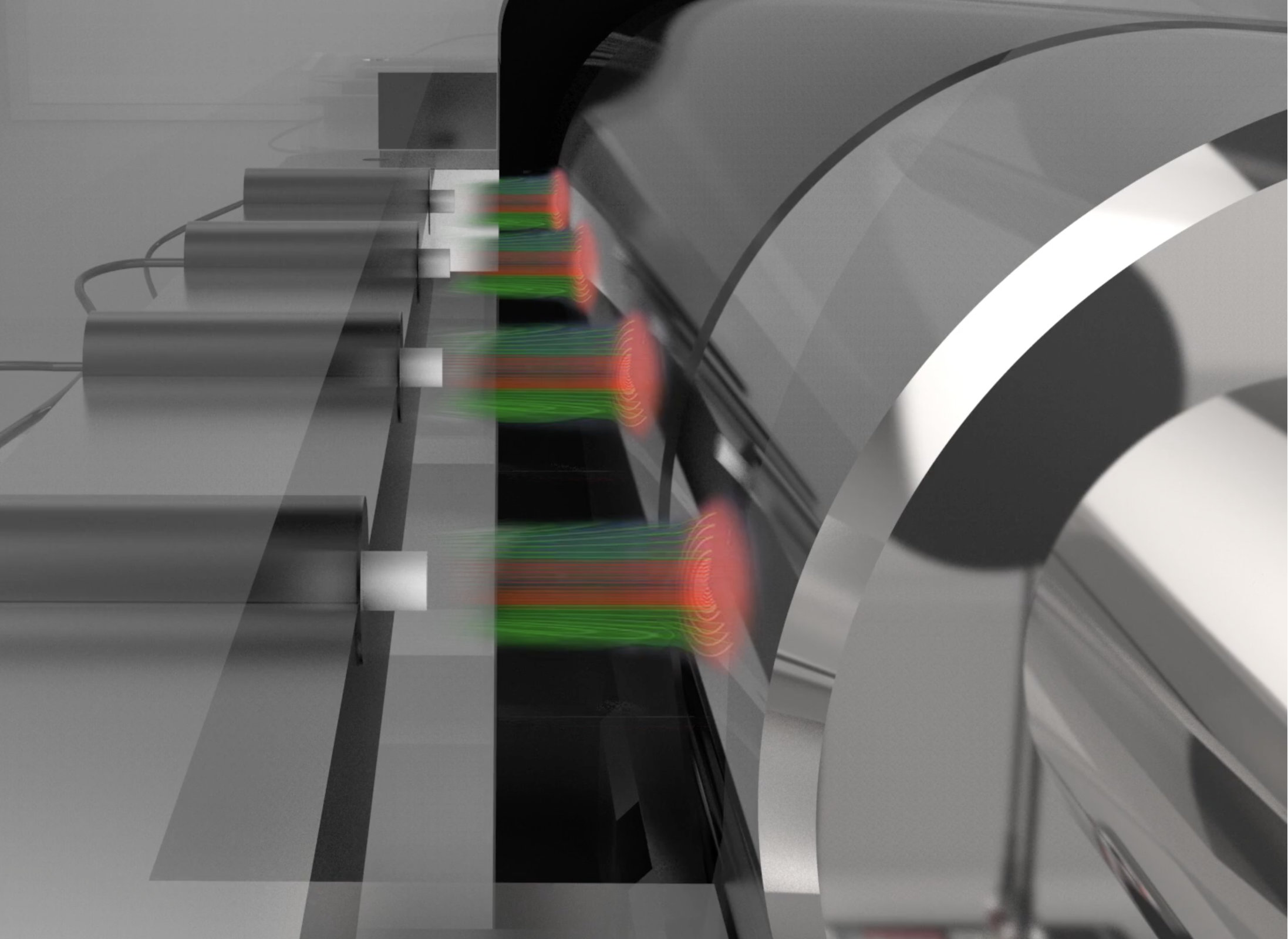
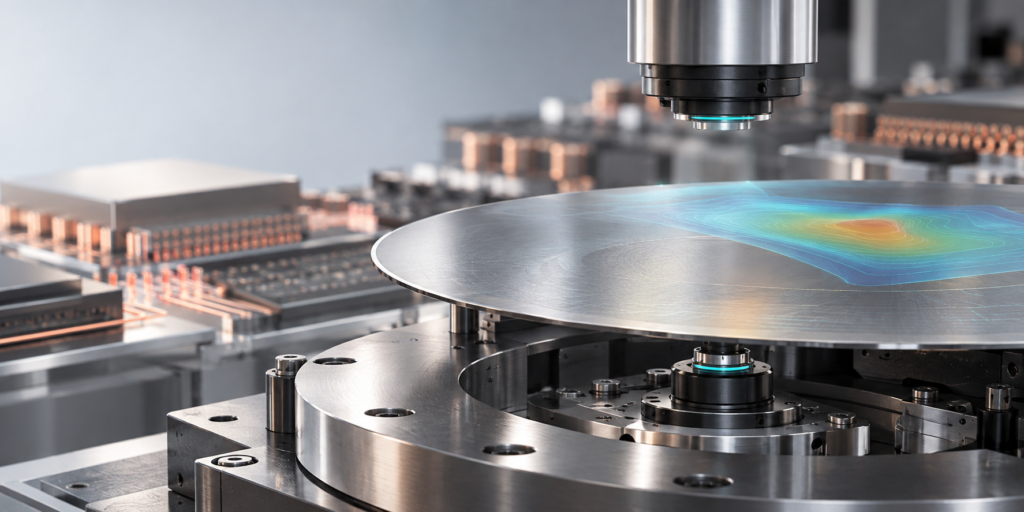
The Proforma systems use MTI’s proprietary Push-Pull capacitance technology to provide non-contact thickness measurements without requiring consistent wafer grounding. This differential measurement approach supports accurate, repeatable measurement across a range of semiconducting and semi-insulating wafer materials.
A manufacturer establishes inspection points after selected backside operations. Depending on the process, these may include:
- Measurement before grinding to establish the starting condition
- Verification after coarse grinding
- Uniformity evaluation after fine grinding
- Final qualified inspection after polishing or stress relief
- Comparison with established process limits before bonding or assembly based thickness measurements.
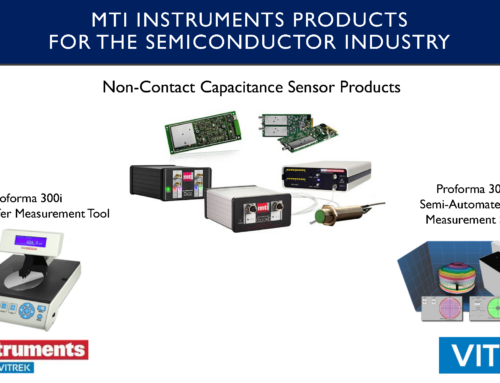
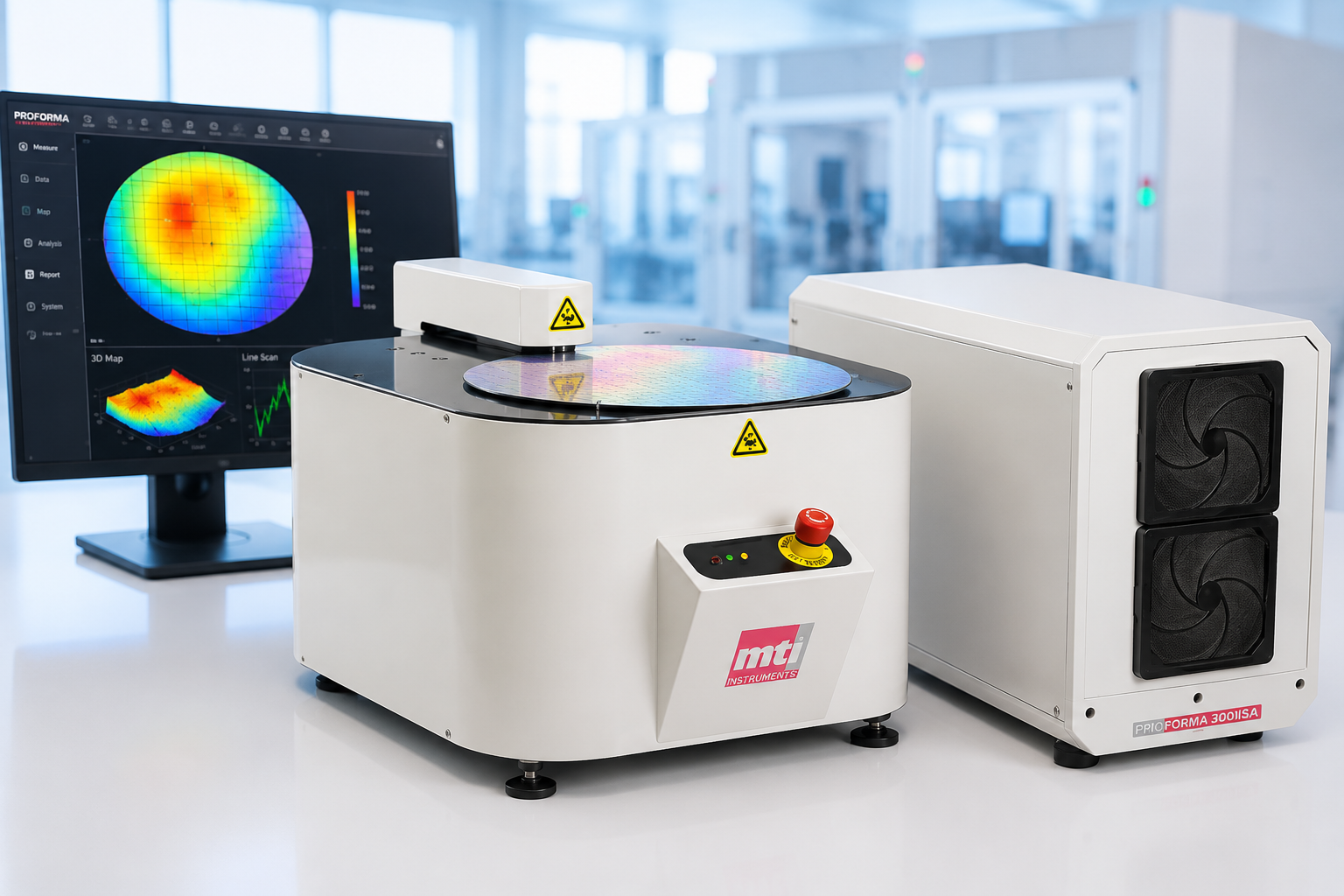
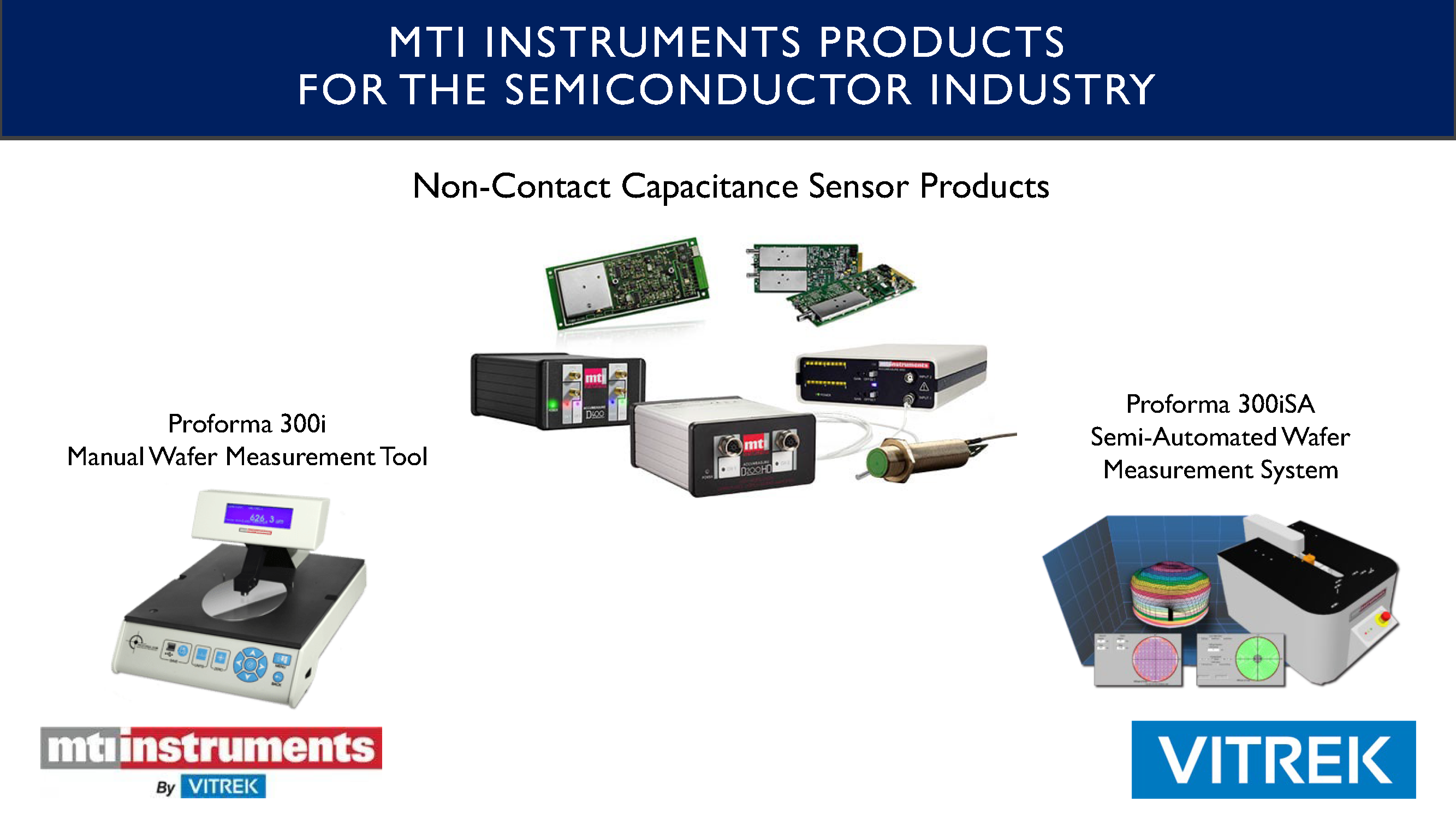
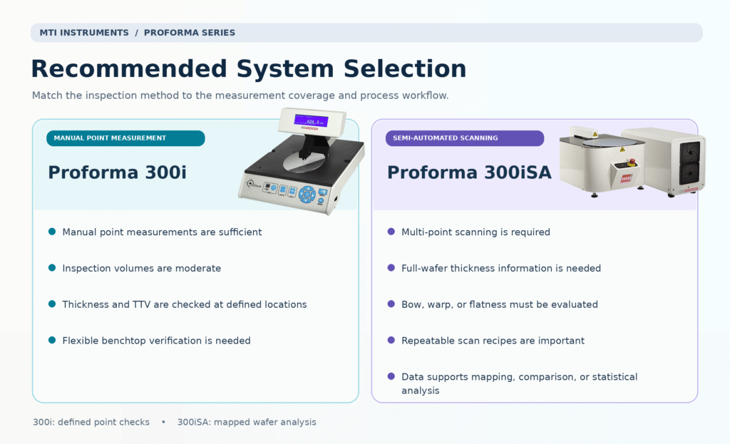
The Proforma 300i provides quick manual thickness checks at defined wafer locations when automated mapping is unnecessary.
The Proforma 300iSA provides semi-automated wafer scanning. Engineers can create measurement routines that collect data at selected locations or across defined wafer regions. The system measures thickness and total thickness variation while also supporting bow, warp, site-flatness and global-flatness analysis.
Published specifications include thickness accuracy of ±0.25 μm and resolution of 0.05 μm. The Proforma 300iSA can collect as many as 1,000 measurement points per minute, depending on the selected routine and system configuration.
Application Example
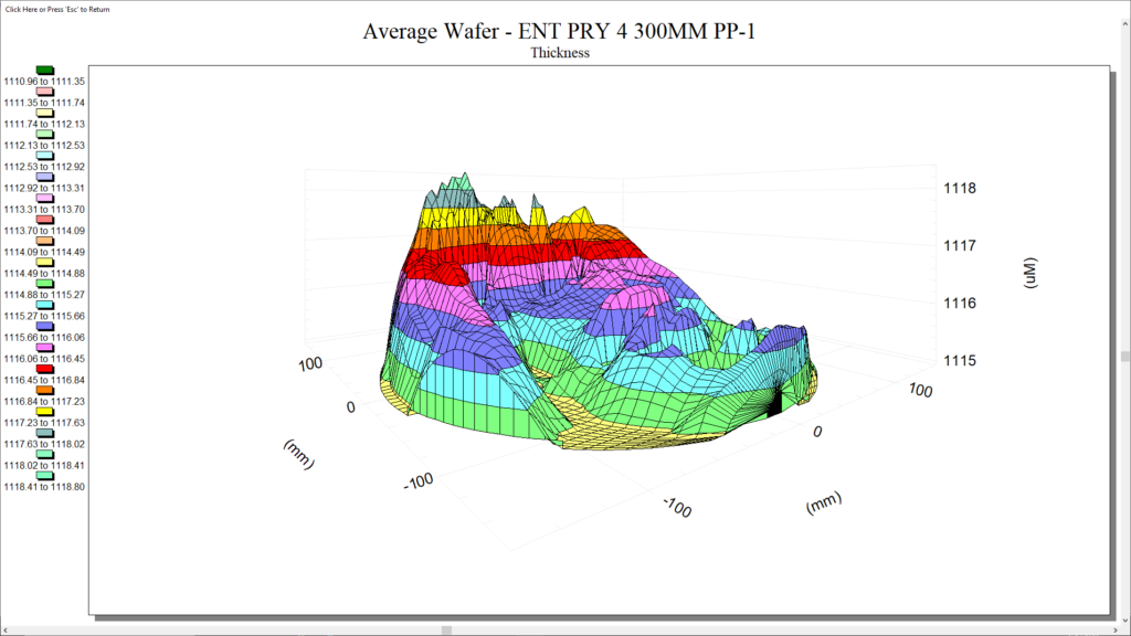
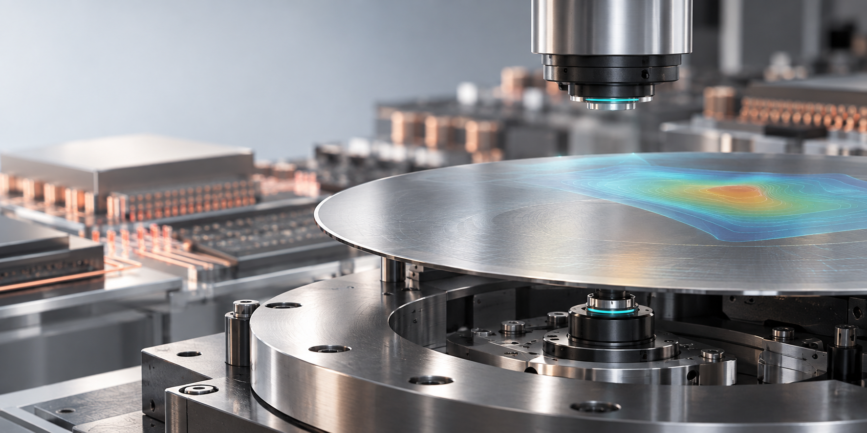
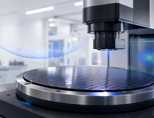
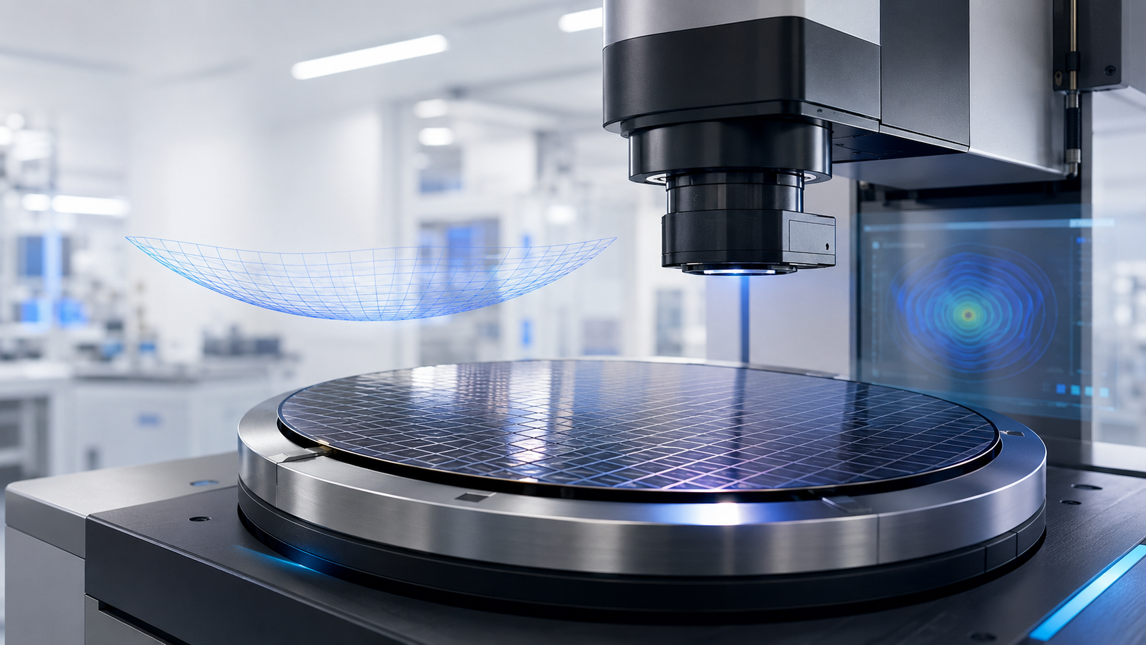
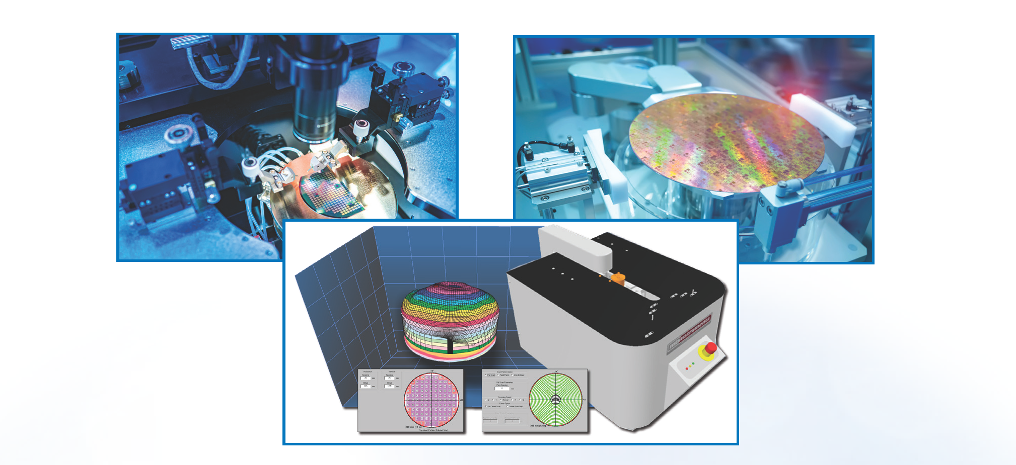
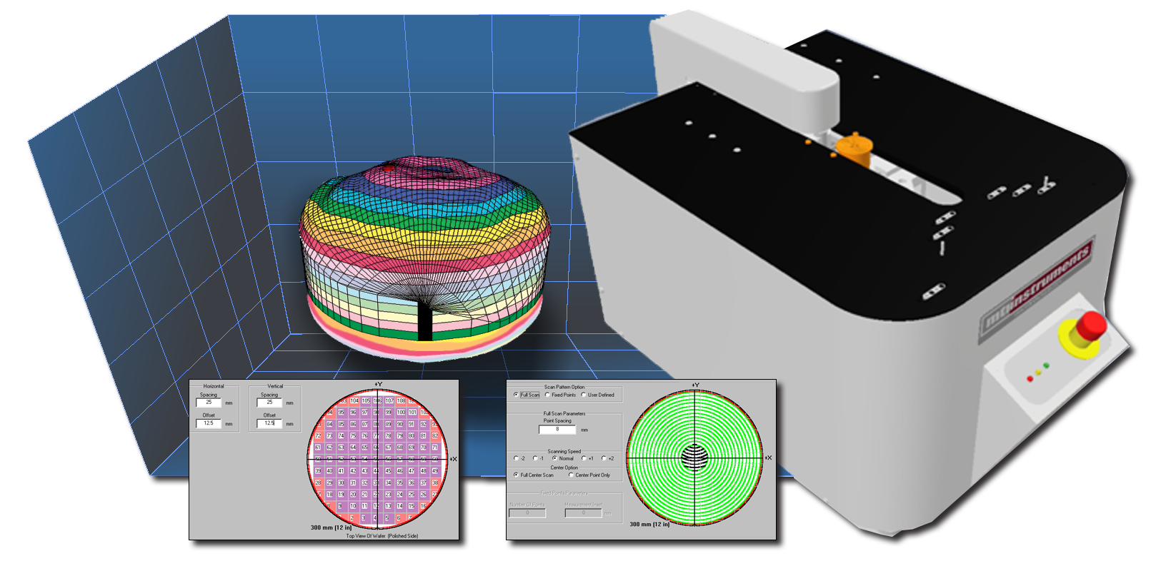
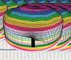
Figure 1. 3-D Wafer Thickness Map. A center-point reading may be within specification while a multi-point scan reveals thinner regions elsewhere on the wafer. The profile shows the corresponding dips in thickness.
A semiconductor manufacturer is preparing wafers for an AI accelerator package incorporating logic and stacked high bandwidth memory.
The wafers enter the backside process at their original substrate thickness. Grinding and polishing are used to move them progressively toward the qualified packaging specification.
After coarse grinding, the operator uses the Proforma system to confirm average thickness and check defined locations a cross the wafer. The measurement shows that material removal remains within the expected process window.
Following fine grinding, the manufacturer performs a more detailed measurement. Mapping reveals that one region is thinner than the remainder of the wafer, even though its center-point thickness remains acceptable.
Because the variation is identified before polishing and package assembly, process engineers can inspect the grinding recipe, wafer support, alignment and equipment condition. Corrective action is completed before the next production lot is processed.
After polishing, a final qualified measurement confirms that the wafer meets the applicable thickness and geometry requirements before it advances to bonding or assembly.
Process Benefits
Using non-contact thickness measurement between backside-processing stages can help manufacturers:
- Detect process drift before final inspection
- Identify localized non-uniformity that a single measurement may miss
- Compare material removal between grinding and polishing operations
- Monitor bow and warp as wafer stiffness decreases
- Reduce operator-dependent measurement variability
- Support process qualification and statistical process control
- Prevent unsuitable wafers from advancing to high-value packaging steps
Application Considerations
The measurement setup must be qualified for the actual wafer and manufacturing process. Important considerations include:
- Wafer material and electrical properties
- Diameter and target thickness
- Surface condition and deposited films
- Carrier, tape or temporary-bonding configuration
- Wafer support and handling method
- Required measurement locations
- Acceptable uncertainty and process limits
- Environmental vibration and temperature
- Data-export and statistical-process-control requirements
Extremely thin wafers may require specialized handling, support or fixturing. The applicable Proforma configuration and qualified thickness range should be confirmed with MTI Instruments for each application.
Conclusion
Backside processing for AI accelerators, HBM and chiplet-based devices requires more than achieving a nominal final thickness. Manufacturers must understand how material is being removed, whether uniformity is changing and whether wafer geometry remains suitable for downstream integration.
The MTI Instruments Proforma 300i and Proforma 300iSA provide non-contact measurement data that can be used at defined process checkpoints. By identifying thickness variation and geometry changes before wafers enter bonding, stacking or assembly, manufacturers can improve process control, reduce scrap risk and protect the considerable value already added to advanced semiconductor devices.
Request a Free Demo
See how the Proforma Series can improve your wafer thickness and flatness testing efficiency. A Vitrek application engineer will follow up within one business day.