
 Transducer Selection for High Resolution Applications Gallery
Transducer Selection for High Resolution Applications
Application Notes-MTI, Brand-MTI, News-MTI-Instrumentation, News-MTI-Metrology, News-Product Updates, News-Products, Products-MTI-Capacitance, Products-MTI-Laser/Fiber Optic, Products-MTI-Semiconductor/Metrology, Products-MTI-Signal Generators, Z-REPUB, z1
Transducer Selection for High Resolution Applications
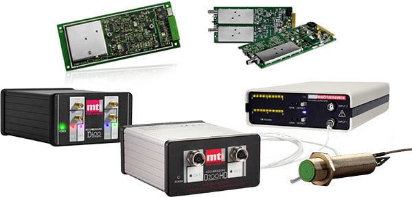
High resolution applications do not always require an interferometer. If you want to make accurate measurements in the micron to picometer range, then an MTI Digital Accumeasure D100 HD or D200 system may be what you need. Laser interferometers can sell for more than $15,000 and be difficult to setup. For example, you may have to buy additional optics to guarantee a good return signal since the laser beam must reflect off a mirror surface or precision retro reflector in order for the beam to re-enter the interferometer’s optics at less than a degree of reflection angle. The downsides [...]
Check Out Vitrek’s Available Education and Product Training Resources
At Vitrek, we do more than just design and build high-quality electrical testing equipment — we ensure that our customers have all of the tools that they need to succeed when using our products. Here, we offer an overview of the plethora of educational resources that we have available on our website. […]
High Resolution Semiconductor Wafer Measurements at Lower Costs
MTI's Proforma technology characterizes semiconductor wafers in terms of bow and warp, thickness, total thickness variation (TTV) and center thickness. Until recently, semiconductor wafer measurements at resolutions less than 100 µm were cost-prohibitive. Moreover, only expensive devices such as interferometers were capable of these measurements. Today, the semiconductor industry can use capacitance gauges instead of laser interferometers to achieve high resolution at fraction of the cost. Much like affordable CCD cameras transformed and expanded the market for video, cost-effective capacitance is disrupting the semiconductor wafer measurement market and creating new opportunities for quality testing and validation. The [...]
Disclaimer
All statements and expressions are the sole opinion of the company and are subject to change without notice. The Company is not liable for any investment decisions by its readers or subscribers. It is strongly recommended that any purchase or sale decision be discussed with a financial advisor, or a broker-dealer, or a member of any financial regulatory bodies. The information contained herein has been provided as an information service only. The accuracy or completeness of the information is not warranted and is only as reliable as the sources from which it was obtained. Investors are cautioned that they may [...]
 Measure Wafer Bow, Warp and TTV with Capacitance Gallery
Measure Wafer Bow, Warp and TTV with Capacitance
Application Notes-MTI, Brand-MTI, Industry-Battery, Industry-Compliance Testing, Industry-Consumer Products, Industry-Electronics, Industry-Manufacturing, Industry-Semiconductor, Industry-Semiconductor-MTI, Industry-Sensors, Products-MTI-Capacitance, Z-REPUB, z1, ZOK

Measure Wafer Bow, Warp and TTV with Capacitance
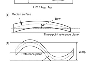
The flatness of silicon wafers used to manufacture integrated circuits is controlled to tight tolerances to help ensure that the whole wafer is sufficiently flat for lithographic processing. To ensure your wafer manufacturing process is within tolerance, you need to measure the wafers being produced. Various measurement techniques exist to verify process tolerances and eliminate expensive scrap wafers. Non-contact capacitive sensing is a highly precise and cost-effective means to measure wafer flatness, bow, warp, and total thickness variation (TTV). MTI Instruments’ Proforma 300i and 300iSA systems use capacitance sensors to improve yields while reducing costs through better dimensional control of [...]
 How to Measure Dielectric Separator Thickness in EV Batteries Gallery
How to Measure Dielectric Separator Thickness in EV Batteries
Application Notes-MTI, Brand-MTI, Industry-Automotive, Industry-Compliance Testing, Industry-Consumer Products, Industry-Electronics, Industry-Government/Military, Industry-Manufacturing, Industry: Transportation, News-MTI, News-MTI-Instrumentation, Products-MTI-Capacitance, Products-MTI-Laser/Fiber Optic, Products-MTI-Signal Generators, Z-REPUB, z1

How to Measure Dielectric Separator Thickness in EV Batteries
The International Energy Agency predicts that as many as 125 million electric vehicles (EVs) will be on the road by 2030. At the heart of these electric cars, trucks, and buses is the lithium-ion (Li-ion) battery, a type of rechargeable battery with high energy density and low self-discharge. The plates in Li-ion batteries consist of lithium compounds that are applied to either a copper plate substrate (cathode) or an aluminum substrate (anode). In turn, these two plates are separated by a dielectric separator. All of the layers in an EV battery are extremely thin. In fact, the cathode and [...]
Privacy Policy
What Do We Do With The Information You Provide? We may ask you to give us contact and demographic information when you register. We use this information to send our Site's users like you information about the Site or Services. We also use this information to contact you both on line and offline when needed. What Do We Do With Your IP Address And Cookies? We use your IP address to help diagnose problems with our server and to administer our website. Your IP address is used to gather broad demographic information and is stored as a partial identifier. [...]
Legacy Products
Vitrek Legacy Products Vitrek 944i Dielectric Analyzer and 930i Ground Bond Tester See 95x This product line has been replaced by the 95x Series. Vitrek V3, V50 & V60 Series (V3, V50, V51, V52, V53, V60, V61, V63, V4) Testers See V7X This product line has been replaced by the V7X Series. Vitrek 4600, 4600A, and 46XXB Series High Voltage Meters See 4700 This product line has been replaced by the 4700 HV Meter. Vitrek 948i High Voltage Switching System See 964i [...]
Capacitance Sensing for Non-Contact Thickness Measurements of Insulating Materials
Capacitance sensing can be used to make non-contact thickness measurements for most insulating materials. Capacitance sensors are known for their ability to precisely measure the thickness and position of conductive targets, but what’s less known is that these sensors can also measure the thickness of non-conductive materials. Examples include glass, sapphire, and plastics, as well as semi-insulating semiconductor materials such as GaAs and silicon nitride. Analog vs. Digital Technologies MTI Instruments, a global supplier of precision measurement technologies, takes the guesswork out of what used to be a complex measurement for non-conductive materials. MTI's Digital Accumeasure system features a [...]