Press Release: Accumeasure Capacitive Wafer Measurement Tools Reduce Start-up Costs for Specialty Fabs & Their Tier Ones
Accumeasure™ Capacitive Wafer Measurement Tools Reduce Start-up Costs for Specialty Fabs & Their Tier Ones Vitrek’s Cost-Sensitive Accumeasure Capacitance-Based Metrology System Simplifies the Development of Adaptable High-Precision Equipment—Especially in USA Lockport, IL — February 5, 2026 — Vitrek, a US-based leader in precision measurement instruments, today announced the expanded capabilities of its MTI Accumeasure Capacitance Technology. Designed to make high-precision wafer metrology more accessible to start-up and smaller niche semiconductor equipment makers, Vitrek’s Accumeasure technology provides a compact, cost-effective alternative to traditional high-end optical systems that are often too bulky or expensive for new market entrants. Key [...]
Press Release: MTI Instruments’ Proforma 300iSA Handles Critical Multi-Material Wafer Inspection for a Rapidly Evolving Industry
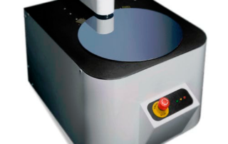
MTI Instruments’ Proforma 300iSA Handles Critical Multi-Material Wafer Inspection for a Rapidly Evolving Industry Universal semi-automated platform measures diverse wafer materials and surfaces with SEMI and ASTM standard compliance. Lockport, IL—20 January 2026-Vitrek announced today that its Proforma 300iSA semi-automated metrology system has proven capable of supporting wafer inspection across a growing range of semiconductor materials, wafer sizes, and surface finishes including silicon (Si), silicon carbide (SiC), gallium arsenide (GaAs), and indium phosphide (InP). Inspection systems are being pushed to handle more various materials and tighter processes as device manufacturers move beyond traditional silicone into compound semiconductors [...]
Press Release: Today’s Wafer Designs Put Premium on Precision— 300i Increases ROI
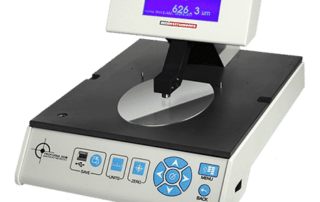
Today’s Wafer Designs Put Premium on Precision— 300i Increases ROI Value of incoming wafer inspection with 300i’s ±0.25µm accuracy far outweighs potential for costly downstream yield losses Lockport, IL, - December 16, 2025- Semiconductor fabrication facilities risk substantial financial exposure from incoming wafers defects. With typical lot sizes of 25 wafers and finished wafer values ranging from $4,000 to $17,000, depending on complexity, a single contaminated lot can translate into $100,000 to $425,000 in processed material losses – plus the costs of production delays, Vitrek’s affordable Proforma 300i manual metrology system, provides the precision needed to insure y [...]
 MTI Application Note: How to Achieve Gallery
MTI Application Note: How to Achieve <1um Accuracy When Measuring Roller Gap
Application Notes-MTI, Brand-MTI, Industry-Compliance Testing, Industry-Consumer Products, Industry-Manufacturing, Industry-Sensors, News-MTI-Metrology, Products-MTI-Capacitance, z1
MTI Application Note: How to Achieve <1um Accuracy When Measuring Roller Gap
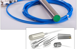
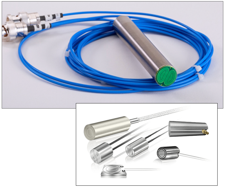
How to Achieve <1um Accuracy When Measuring Roller Gap Roller Gap Measurement with MTI Digital Accumeasure Capacitive Probes Many roll-to-roll finishing processes typically use a calender, or series of hard pressure rollers, to deliver smooth, high-quality products of plastic, textile, or paper (Fig 1). Ensuring a consistent material thickness, however, depends on the ability to monitor, and maintain, a precise gap between rollers. This application note describes a quick and easy means for roller gap measurement. Problem How to measure the small gap between rollers to keep track of product thickness. Typically, it’s not possible to [...]
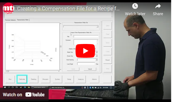
 Creating a Compensation File for a Recipe for the Proforma 300iSA – Video Gallery
Creating a Compensation File for a Recipe for the Proforma 300iSA – Video
Brand-MTI, Industry-Compliance Testing, Industry-Electronics, Industry-Manufacturing, Industry-Semiconductor, Industry-Semiconductor-MTI, Industry-Semiconductor-Videos, News-MTI-Metrology, Products-MTI-Semiconductor/Metrology, Videos-MTI-Manual Semiconductor Metrology System, Videos-MTI-Semiautomated Metrology System, z1

 A Comprehensive Guide to Non-Contact Sensors and Their Applications Gallery
A Comprehensive Guide to Non-Contact Sensors and Their Applications
Application Notes-MTI, Articles-MTI, Brand-MTI, Industry-Sensors, News-MTI-Metrology, Products-MTI-Capacitance, Products-MTI-Laser/Fiber Optic, Products-MTI-Semiconductor/Metrology, Whitepapers-MTI, Z-REPUB, z1
A Comprehensive Guide to Non-Contact Sensors and Their Applications
Sensors, both contact and non-contact, are crucial devices that allow the monitoring, detection, and reaction to conditions in an environment or within a process or piece of equipment. While myriad types of sensors exist and are designed to monitor varying conditions, all of them can be characterized as being one of two types — contact sensors and non-contact sensors. We’ll focus on the latter, diving into different technologies, types, and applications of non-contact sensor technology; but first, let’s explore what differentiates contact and non-contact sensors. Contact vs. Non-Contact Sensors: What’s the Difference? Measuring, monitoring, or detecting a particular condition [...]
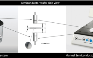
 The Benefits of Manual, Semi-Automated, and Fully-Automated Systems for Semiconductor Wafer Inspection and Metrology Gallery
The Benefits of Manual, Semi-Automated, and Fully-Automated Systems for Semiconductor Wafer Inspection and Metrology
Application Notes-MTI, Brand-MTI, Industry-Consumer Products, Industry-Electronics, Industry-Manufacturing, Industry-Semiconductor, Industry-Semiconductor-MTI, News-MTI-Metrology, Products-MTI-Semiconductor/Metrology, z1
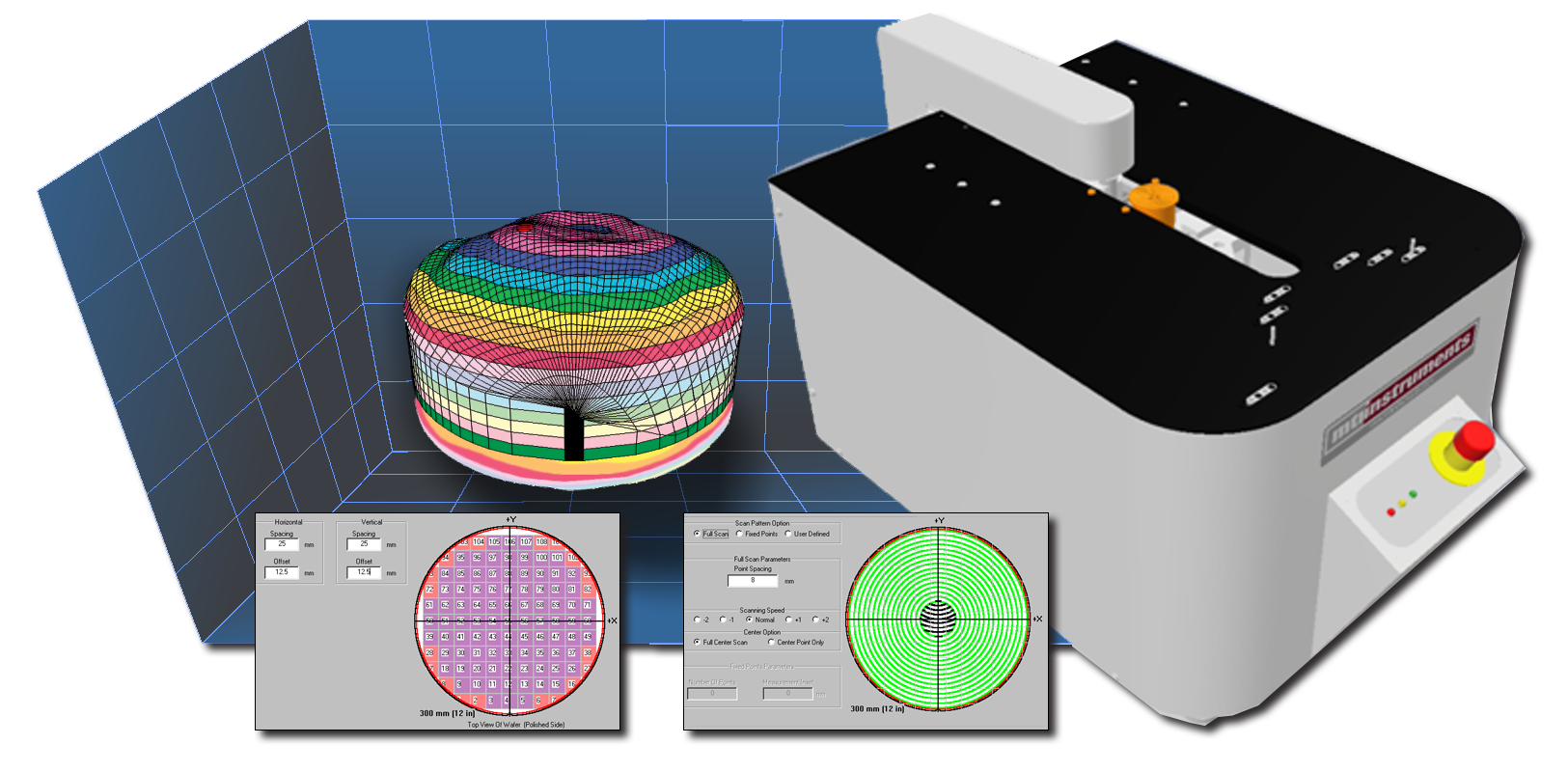
The Benefits of Manual, Semi-Automated, and Fully-Automated Systems for Semiconductor Wafer Inspection and Metrology
This is the third of three articles in Semiconductor Wafer Measurement for Increased Profitability. The first article in this series explains why disc geometry matters. The second article examines the cost of failing to inspect semiconductor wafers. Fully automated systems that can load, scan, and unload wafers are fast, convenient, and efficient at high volumes. They’re useful for checking every wafer in every batch, but these systems are expensive. Semi-automated and manual systems cost significantly less and are generally used for lower volumes; however, they’re also easy-to-use and can make fast, accurate measurements that support production flow. Semi-automated and [...]
 Why Disc Geometry Matters In Wafer Production Gallery
Why Disc Geometry Matters In Wafer Production
Application Notes-MTI, Brand-MTI, Industry-Consumer Products, Industry-Electronics, Industry-Manufacturing, Industry-Semiconductor, Industry-Semiconductor-MTI, News-MTI-Metrology, Products-MTI-Semiconductor/Metrology, z1
Why Disc Geometry Matters In Wafer Production
This is the first of three articles in Semiconductor Wafer Measurement for Increased Profitability. The second article examines the cost of failing to inspect semiconductor wafers. The third article describes the benefits of using semi-automated, fully-automated, and manual systems for wafer metrology and inspection. Semiconductor wafers are cut from cylindrical silicon crystals, or ingots. The flatness of these disc-shaped wafers is controlled to tight tolerances to ensure that the entire wafer surface is suitable for integrated circuit (IC) production. If disc geometry is out-of-spec after cutting, it may be possible to reprocess the wafer. Cutting is only the first [...]
 Why Demand for SiC Wafers is Soaring and Durable Gallery
Why Demand for SiC Wafers is Soaring and Durable
Brand-MTI, Industry-Consumer Products, Industry-Electronics, Industry-Manufacturing, Industry-Semiconductor, Industry-Semiconductor-MTI, MTI Blog, News-MTI, News-MTI-Metrology, Products-MTI-Semiconductor/Metrology, Z-REPUB, z1
Why Demand for SiC Wafers is Soaring and Durable
Silicon carbide (SiC) wafers are in high demand, particularly in high-temperature applications. Silicon carbide (SiC), a semiconductor material made of both silicon and carbon, can withstand extreme temperatures of up to 2700°C. Often referred to as carborundum, SiC’s unique properties also make it a key material in non-electronic applications such as bulletproof vests, extrusion dies, sandpaper, and high-performance disc brakes. In the electronics industry, SiC wafers are crucial for devices operating under high temperatures, high voltages, or both. For example, they are used in electric vehicle (EV) power electronics, 5G communication systems, and LED technology, making SiC a material [...]