
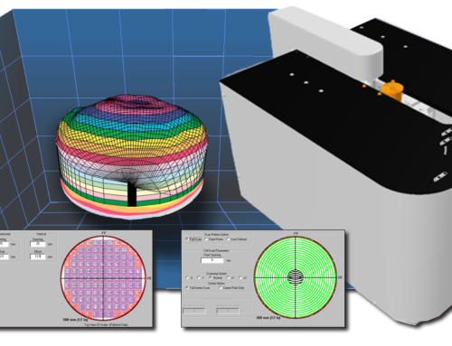
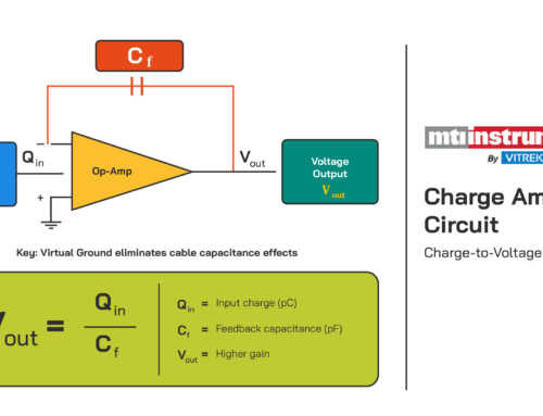
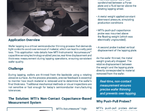
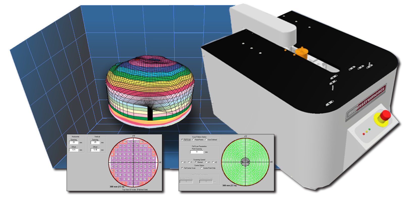
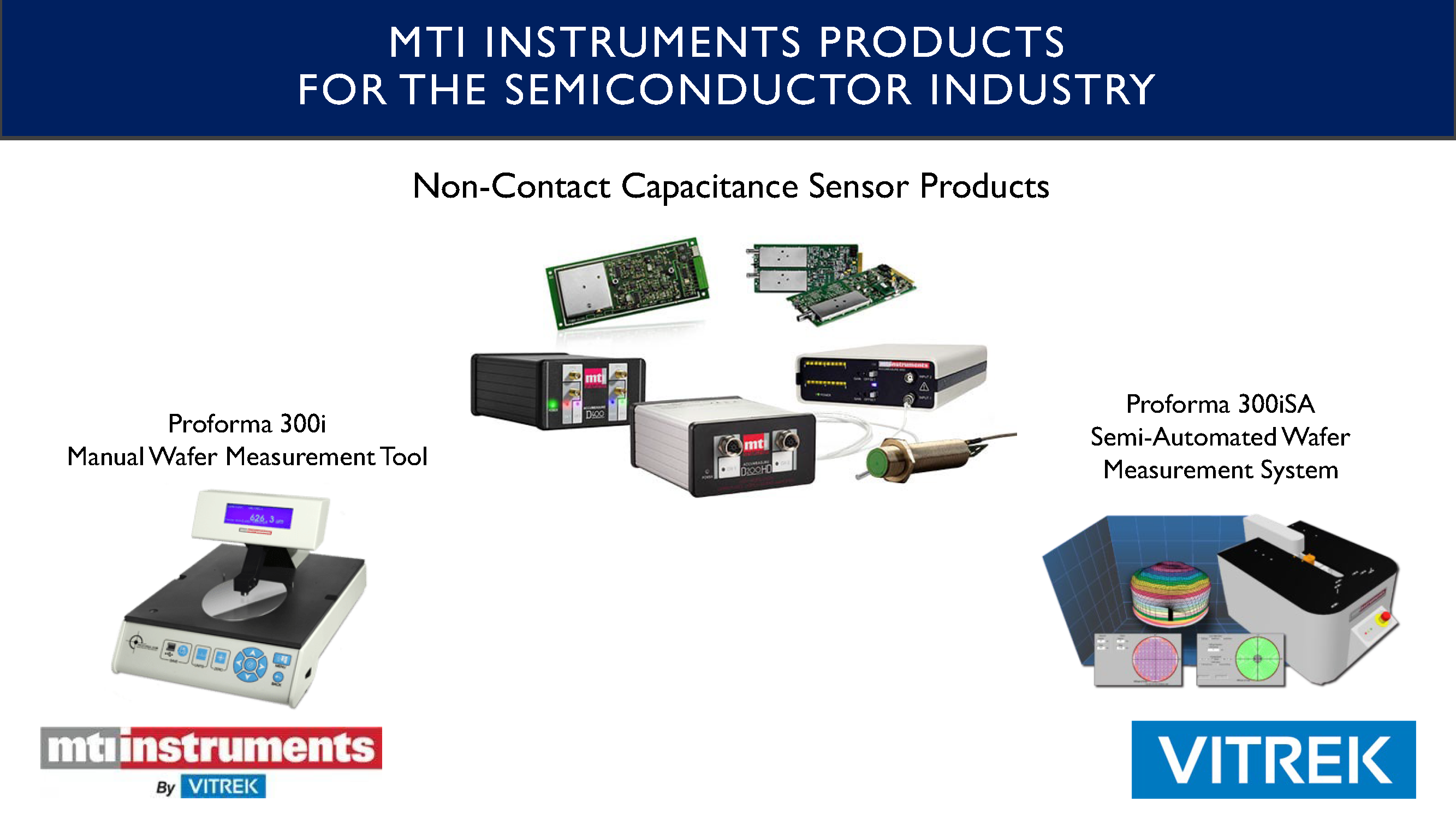
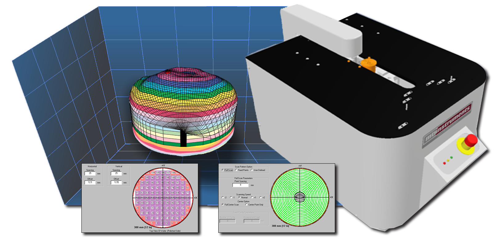
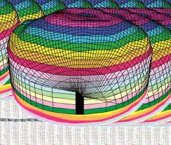
MTI’s Proforma technology characterizes semiconductor wafers in terms of bow and warp, thickness, total thickness variation (TTV) and center thickness.
Until recently, semiconductor wafer measurements at resolutions less than 100 µm were cost-prohibitive. Moreover, only expensive devices such as interferometers were capable of these measurements. Today, the semiconductor industry can use capacitance gauges instead of laser interferometers to achieve high resolution at fraction of the cost. Much like affordable CCD cameras transformed and expanded the market for video, cost-effective capacitance is disrupting the semiconductor wafer measurement market and creating new opportunities for quality testing and validation. The benefits also include less waste, greater yield and as a result, faster return on investment (ROI).
Only the Complexity is Free
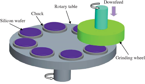
Semiconductor wafer measurement is complex because of the way individual wafers are made. To produce integrated circuits (ICs), a semiconductor material such as silicon is grown and then cut and polished. A negative pattern of IC traces is then imprinted on a reticle. During lithography, light shines through the reticle onto the wafer. Because the distance from the reticle to the wafer requires tight tolerances, variations in the wafer’s surface must not exceed a few microns. Semiconductor wafers are never perfectly flat, but one that is not flat enough is unusable.
At a microscopic level, a wafer’s surface topology resembles a potato chip or a sombrero, depending on your preferred analogy. This undulation, or bow and warp, is just one of several wafer measurements that are taken. Before lithography occurs, it is important to measure thickness, total thickness variation (TTV) and center thickness. Otherwise, the monetary value that is added to the wafer through patterning can become a form of manufacturing waste. Semiconductor wafers vary in cost, but a finished 300 mm wafer can be worth thousands of dollars. Across many wafers, the cost of this waste can become significant.
Capacitance Gauges vs. Laser Interferometers
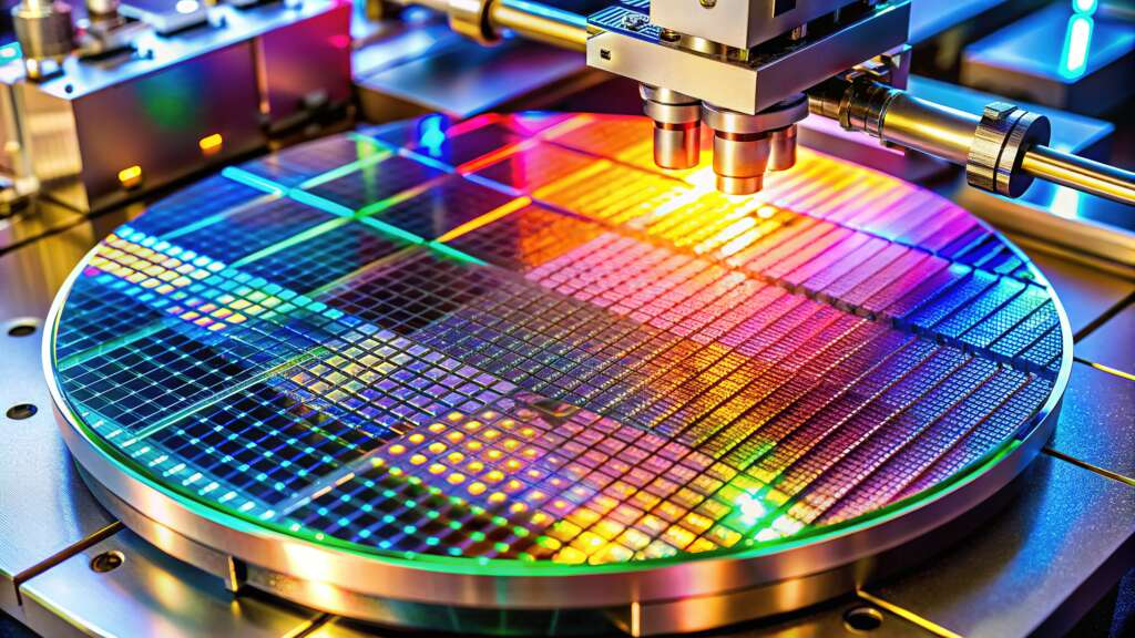
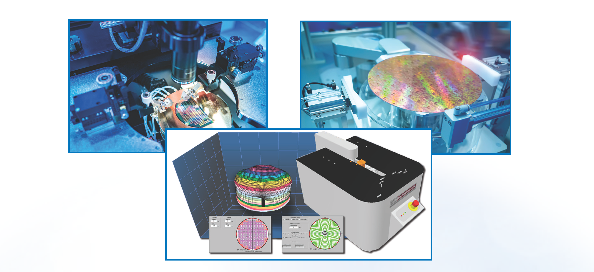
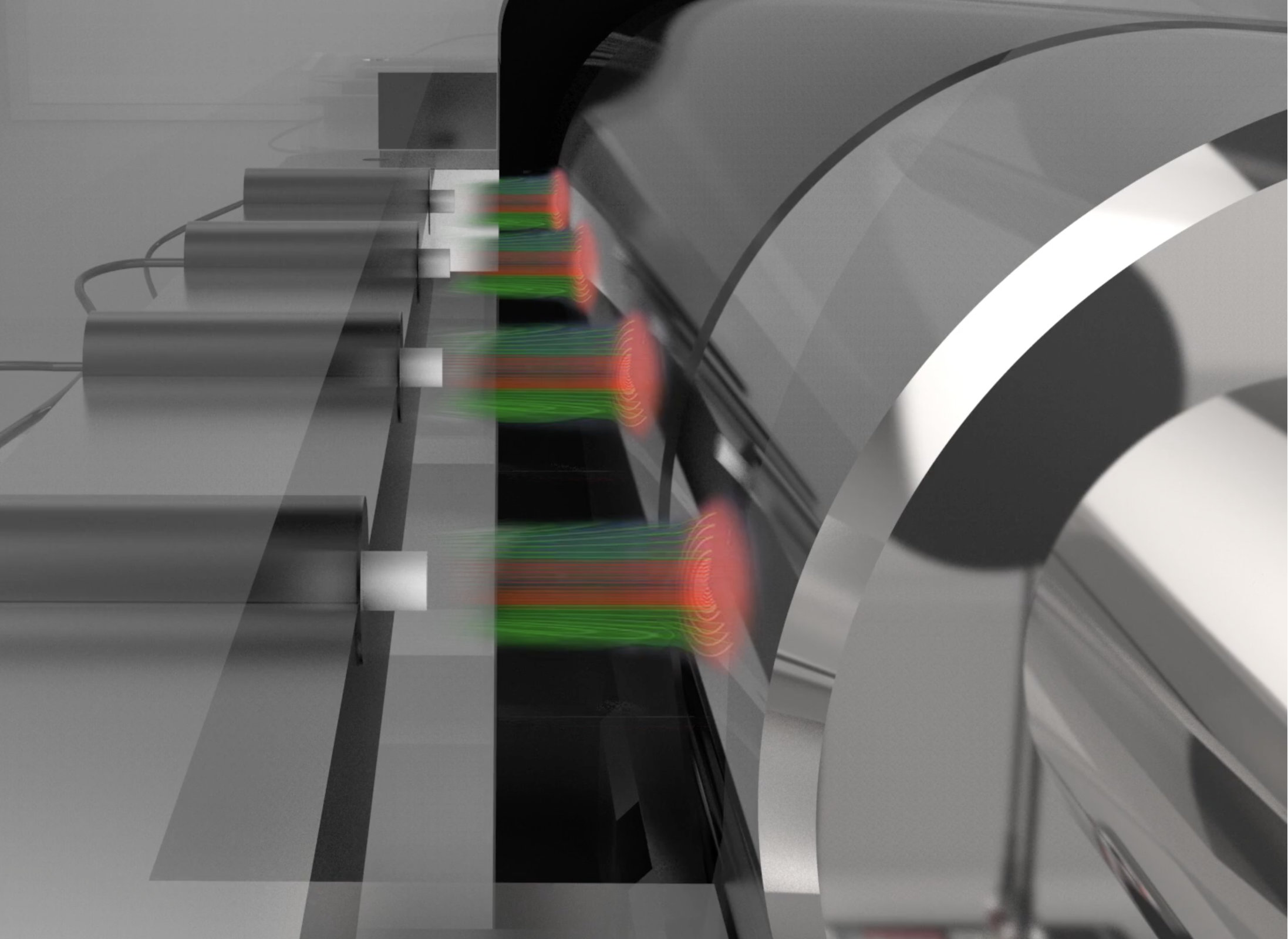
Semiconductor Manufacturing: Front View of Silicon Wafer in Photolithography Process
Laser interferometers are used to make high-resolution measurements, but these high-end devices cost significantly more than capacitance gauges. Plus, laser interferometers provide relative readings. That means an operator must calibrate the device to a known thickness before use. The operator can observe the change in height after measurement begins, but the height of the starting point remains unknown. By contrast, capacitance gauges provide absolute measurements instead of relative ones for greater absolute accuracy. Optical technologies are at a disadvantage in other ways, too.
If a laser interferometer loses track of the wafer’s surface, the resulting measurement is inaccurate. By contrast, non-contact capacitance probes like the ones made by MTI Instruments use spatial averaging. In other words, MTI’s capacitance-based technologies take measurements over a larger area and then calculate the average. This eliminates the microscopic optical effects caused by surface contamination that is invisible to the human eye. With laser interferometers, measuring transparent or translucent semiconductor wafers is also challenging. Here, capacitance gauging is also a better choice.
Over time, laser sensors have a tendency to drift respective to temperature, thermal heating, and other factors. Because lasers are a form of light, they can cause the electronic circuitry in interferometers to drift. Capacitance circuits tend to be more stable and combine low drift with high accuracy. For semiconductor manufacturers with multiple facilities, it’s important for the same instrument in different locations to work the same way. Otherwise, data that’s exchanged between facilities won’t correlate. Eyeballing a wafer won’t tell you if it’s out of tolerance, so the industry needs to trust its tools.
In-Line and Off-Line Tools for Semiconductor Wafer Measurement Applications
In-line measurement tools are highly accurate but very expensive. Although they serve an important purpose for quality control, it is unprofitable to identify out-of-tolerance wafers after they’ve been patterned. MTI Instruments’ Proforma 300i and 300iSA systems are off-line measurement tools that cost less and support quality checks earlier in the manufacturing process. MTI’s capacitance-based systems can also expand the applications for quality control across the semiconductor supply chain.
For example, companies that make wire saws can use MTI’s Proforma technology to qualify their machines by measuring wafers after cutting. Companies that make lapping machines or lithography tools can also use Proforma 300i or 300iSA systems for equipment qualification. Just as a vendor that sells wafers can perform high-resolution measurements before shipping them, customers who buy wafers can use Proforma’s off-line measurements upon receipt. This technology also supports research and development projects (R&D) and can be used to calibrate in-line equipment.
All semiconductor manufacturers want to reduce waste. Startups need to define their procedures. Mature companies have processes in-place but still need to calibrate equipment, tackle R&D projects, and pursue continuous improvement. MTI Instruments’ Proforma 300i and 300iSA can measure wafer thickness, bow and warp, TTV and center thickness at high resolution. These systems cost significantly less than laser interferometers and have an accuracy of ±0.25 µm and a resolution of ±0.05 µm. They are used with materials that include silicon, silicon carbide, gallium-arsenide, indium-phosphide and sapphire and tape.
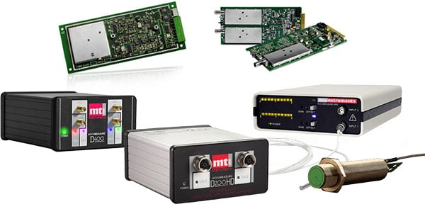
MTI’s Digital Accumeasure can also be used to measure the thickness of semiconductor. This capacitance-based system uses a special dielectric mode of operation to provide highly accurate thickness measurements that are typically less than a micron. With the Digital Accumeasure, calibration is easy and digital filtering is user-adjustable and selectable. Moreover, thickness measurements can be sent to a standard PC running MTI’s Digital Accumeasure display program.
For more information about semiconductor wafer measurement for high resolution and lower costs, contact MTI Instruments.


