
WAFER QA/QC AFTER SLICING AND POLISHING
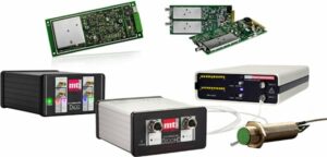
Industry Semiconductor Applications Wafer Qa/Qc After Slicing And Polishing Measurement Type Surface Description When wafers are sliced up with wire saws, they are measured to make sure they are within the specified thickness, with minimal bow, warp, and TTV. After initial measurement, they are sorted and sent for polishing. Since polishing removes material and smoothes out the rough surfaces they need to be measured again to ensure they meet thickness guidelines and quality standards. Solution: MTI Instruments manufactures multiple systems to perform thickness measurements. From semi automated Proforma 300SA to manual wafer [...]
ABOUT WAFER BOW AND WARP MEASUREMENT SYSTEMS
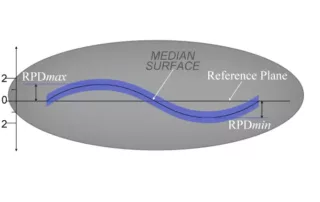
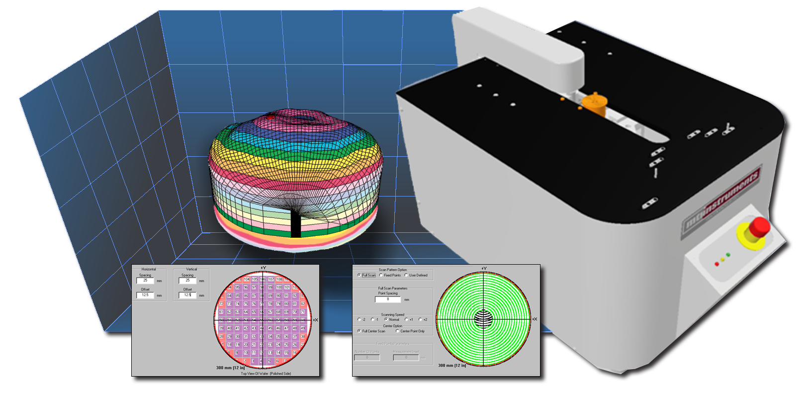
Thickness Measurement for Metrology Systems ASTM F657: The distance through a wafer between corresponding points on the front and back surface. Thickness is expressed in microns or mils (thousandths of an inch). Total Thickness Variation (TTV) ASTM F657: The difference between the maximum and minimum values of thickness encountered during a scan pattern or series of point measurements. TTV is expressed in microns or mils (thousandths of an inch). ASTM F534 3.1.2: The deviation of the center point of the median surface of a free, unclamped wafer from the median [...]
GAAS SUBSTRATE THICKNESS MEASUREMENT
Industry Semiconductor Applications Gaas Substrate Thickness Measurement Measurement Type Thickness Description Measuring Thickness of Wafers with Different Chemistries Introduction: Silicon wafers are ordinarily highly conductive and easy to measure with standard capacitive displacement sensors (See MTI’s Proforma 300i). Measuring the thickness of GaAs wafers that have high bulk resistivity (>10k Ohm/cm) is a little more difficult because the wafers act as non-conductive insulators in a capacitive sensor’s measuring field. Fortunately, MTI has a solution to this problem. Solution: It’s possible to measure the thickness and TTV of high resistivity semiconducting wafers (like GaAs) using non-contact capacitive [...]
MTI Video: Wafer Inspection and Metrology Tutorial (Proforma 300i)
https://www.youtube.com/watch?v=nGkbpG2sz_k Learn More Download this brochure to learn more about the Proforma 300i wafer measurement system for semiconducting and semi-insulating wafers. This article in AZO Sensors also provides information.
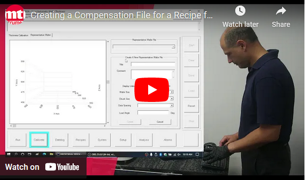
 Creating a Compensation File for a Recipe for the Proforma 300iSA – Video Gallery
Creating a Compensation File for a Recipe for the Proforma 300iSA – Video
Brand-MTI, Industry-Compliance Testing, Industry-Electronics, Industry-Manufacturing, Industry-Semiconductor, Industry-Semiconductor-MTI, Industry-Semiconductor-Videos, News-MTI-Metrology, Products-MTI-Semiconductor/Metrology, Videos-MTI-Manual Semiconductor Metrology System, Videos-MTI-Semiautomated Metrology System, z1

 A Comprehensive Guide to Non-Contact Sensors and Their Applications Gallery
A Comprehensive Guide to Non-Contact Sensors and Their Applications
Application Notes-MTI, Articles-MTI, Brand-MTI, Industry-Sensors, News-MTI-Metrology, Products-MTI-Capacitance, Products-MTI-Laser/Fiber Optic, Products-MTI-Semiconductor/Metrology, Whitepapers-MTI, Z-REPUB, z1
A Comprehensive Guide to Non-Contact Sensors and Their Applications
Sensors, both contact and non-contact, are crucial devices that allow the monitoring, detection, and reaction to conditions in an environment or within a process or piece of equipment. While myriad types of sensors exist and are designed to monitor varying conditions, all of them can be characterized as being one of two types — contact sensors and non-contact sensors. We’ll focus on the latter, diving into different technologies, types, and applications of non-contact sensor technology; but first, let’s explore what differentiates contact and non-contact sensors. Contact vs. Non-Contact Sensors: What’s the Difference? Measuring, monitoring, or detecting a particular condition [...]
 The Benefits of Manual, Semi-Automated, and Fully-Automated Systems for Semiconductor Wafer Inspection and Metrology Gallery
The Benefits of Manual, Semi-Automated, and Fully-Automated Systems for Semiconductor Wafer Inspection and Metrology
Application Notes-MTI, Brand-MTI, Industry-Consumer Products, Industry-Electronics, Industry-Manufacturing, Industry-Semiconductor, Industry-Semiconductor-MTI, News-MTI-Metrology, Products-MTI-Semiconductor/Metrology, z1
The Benefits of Manual, Semi-Automated, and Fully-Automated Systems for Semiconductor Wafer Inspection and Metrology
This is the third of three articles in Semiconductor Wafer Measurement for Increased Profitability. The first article in this series explains why disc geometry matters. The second article examines the cost of failing to inspect semiconductor wafers. Fully automated systems that can load, scan, and unload wafers are fast, convenient, and efficient at high volumes. They’re useful for checking every wafer in every batch, but these systems are expensive. Semi-automated and manual systems cost significantly less and are generally used for lower volumes; however, they’re also easy-to-use and can make fast, accurate measurements that support production flow. Semi-automated and [...]