
MEMS-Based High Throughput Screening
MEMS-Based High Throughput Screening Customer Case The customer needs to do frequency analysis to determine the resonant frequency of an oscillating micro-fabricated device. They will use a Laser Doppler Vibrometer to monitor the physical oscillation. This is an instrument that looks at the light reflected from the surface of a moving part to determine the velocity or relative position of the part. Analysis of the motion as a function of the driving frequency determines the resonant frequency. Upon excitation at the resonant frequency, the motion is at its maximum. The expected resonant frequencies are on the order of 1 [...]
Automatic Accelerometer Calibration System
Automatic Accelerometer Calibration System Customer Case The customer's Automated Accelerometer Calibration System provides NIST traceable calibration of most accelerometer types, whether self-generating piezo-electric or accelerometers requiring current or voltage excitation. The output of the accelerometer can be charge or voltage, single- ended or differential, AC or DC coupled, isolated or grounded. In building the automatic calibration system, the need is for optimum versatility with regards to the data acquisition card. LabVIEW is the desired control software, and Signal to Noise Ratio and high vertical resolution is of utmost importance for the small variations that occur in Vibration and Shock [...]
 Contact vs. Non-Contact Measurement and Linear Displacement Sensors Gallery
Contact vs. Non-Contact Measurement and Linear Displacement Sensors
Application Notes-MTI, Brand-MTI, Industry-Compliance Testing, Industry-Consumer Products, Industry-Electronics, Industry-Manufacturing, Industry-Semiconductor, Industry-Semiconductor-MTI, Industry-Sensors, Products-MTI-Capacitance, Z-REPUB, z1, ZOK
Contact vs. Non-Contact Measurement and Linear Displacement Sensors
Contact vs. Non-Contact Measurements Choosing between a contact measurement system and a non-contact measurement system requires careful evaluation of your application’s performance needs, material properties, environmental conditions, and measurement goals. Each system type offers unique advantages- and understanding these distinctions can help you make a more informed decision. Let's explores how contact and non-contact measurement techniques work, their strengths and limitations, and where they’re best applied. What Are Contact Measurement Systems? Contact measurement systems involve tools and sensors that physically touch the object to determine various physical characteristics. These systems are widely used in dimensional metrology, offering high precision, [...]
Deep PCI Capture of Fast Charge-Couple Device (CCD) Array Data
Deep PCI Capture of Fast Charge-Couple Device (CCD) Array Data Customer Case A customer wants to digitize data from a 256x256 infrared charge-couple device (CCD) array. The array data is clocked at 4 MHz through two output channels. Exactly two clock cycles occur between 12-bit line signals, and a dozen or more clock cycles occur between successive frames. The customer wants to digitize the data for a minute or more. Since light level signals from the array can vary widely in amplitude, 12-bit resolution is required. GaGe Case Solution The customer will use the CompuScope 512/PCI with the External [...]

Capacitance Sensors vs. Eddy Current Sensors Application Note
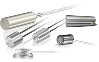
Capacitance Sensors vs. Eddy Current Sensors Application Note Capacitance sensors and Eddy current sensors are both used for non-contact measurements. Capacitive probes use electric fields to measure the distance from the sensor face to the surface of a target that is typically conductive and grounded. Eddy current probes use an alternating AC current to induce a magnetic field in a conductive target instead. In turn, the induced magnetic field produces a back magnetic field that is proportional to the gap between the probe face and the target. In a recent application note, MTI Instruments examines the differences between capacitance [...]
Foam Density Measurement: Capacitance Sensors vs. Nuclear Gauges
This application note from MTI Instruments compares two technologies for measuring foam density: capacitance sensors and nuclear gauges. It examines the basic operating principles of each technology and explains why capacitance measurement is recommended for in-line measurement during foam manufacturing. Capacitance Sensors Capacitive probes are non-contact devices that use electric fields to measure foam density. In combination with a thickness value, a density measurement may be calculated. These probes consist of a capacitance sensor inside of a protective housing and are part of a larger measurement system that includes amplifiers, cables, and software. With parallel plate capacitance, the capacitance probe [...]
Medical
Medical The following example case studies demonstrate how GaGe products and services have been successfully applied in various data acquisition medical applications. We encourage you to contact us and discuss your application in more detail with our engineering team. GaGe can provide tailored custom hardware and software solutions to meet specific application requirements. Did You Know? GaGe Digitizers in Medical Applications View Article Did You Know? GaGe Digitizers in Imaging & Ultrasound Applications View Article Did You Know? GaGe Digitizers in Cancer & Diagnostic Applications View Article Did You Know? [...]
Laser Scanning for Eye Diseases
Laser Scanning for Eye Diseases Customer Case In scanning for non-ablative eye diseases, the customer has a requirement for high vertical resolution while remaining cost effective. By shooting a low-powered laser into the eye (low enough to not cause lasting damage), they are able to determine whether there are any problems in the eye cells. The laser does cause minute damage that is repaired by the antibodies of the eye. The requirement is to capture laser reflections and analyze them. The scan takes place over the entire eye and there are therefore multiple acquisitions. The main obstacle is that [...]
Get More Out Of Your Military & Aerospace Applications
When testing the electrical systems for your military and aerospace applications, you need to ensure they are ready for the job and meet all the necessary standards. These specialized systems work to keep the highly sophisticated and advanced technology housed in these applications running at full strength, which requires the right amount of power to do their jobs effectively. Having the right electrical safety and performance testing equipment on hand can help determine the overall effectiveness of your applications. […]
Echocardiography Experiment
Echocardiography Experiment Customer Case This customer is involved in an Echocardiography experiment. The customer already has an ultrasound imager with a built-in A/D converter which can output 12-bit image data which must be analyzed with the customer's proprietary algorithms on a PC platform. In order to accomplish this, it is required to bring 12-bit digital data at 35 MHz clock rate into a PC. This data is arriving in a burst mode with a repeat frequency of 12.8 KHz with 1000 samples arriving in 28 us followed by no data for the next 50 us. There are 512 such [...]