Thin Film Thickness Measurement Using Capacitance in the Semiconductor Industry
In the semiconductor industry, the precise measurement of thin film thickness is crucial for ensuring the quality and functionality of wafer coatings. Thin films are deposited onto silicon and other wafer materials one atomic layer at a time, and the thickness of these coatings significantly impacts the wafer’s electrical, optical, and mechanical properties. Thin film thickness measurement is particularly important for semiconductor wafers, which may have either conductive metallic films or non-conductive metal oxide films deposited onto them. Common deposition methods include chemical vapor deposition (CVD) and physical vapor deposition (PVD), each employing various processes to apply thin films. 
Given the ultra-thin nature of these coatings, accurate thin film thickness measurement requires highly precise and reliable methods. Without proper measurement, thickness variances can go undetected, leading to further processing and increased manufacturing waste. While several methods exist for gauging thin film thickness, capacitance-based measurement offers distinct advantages, such as its ability to measure non-conductive films, its non-destructive nature, and its speed and ease of use, with high throughput—up to 20 wafers per hour.
Why Choose Capacitance for Thin Film Thickness Measurement?
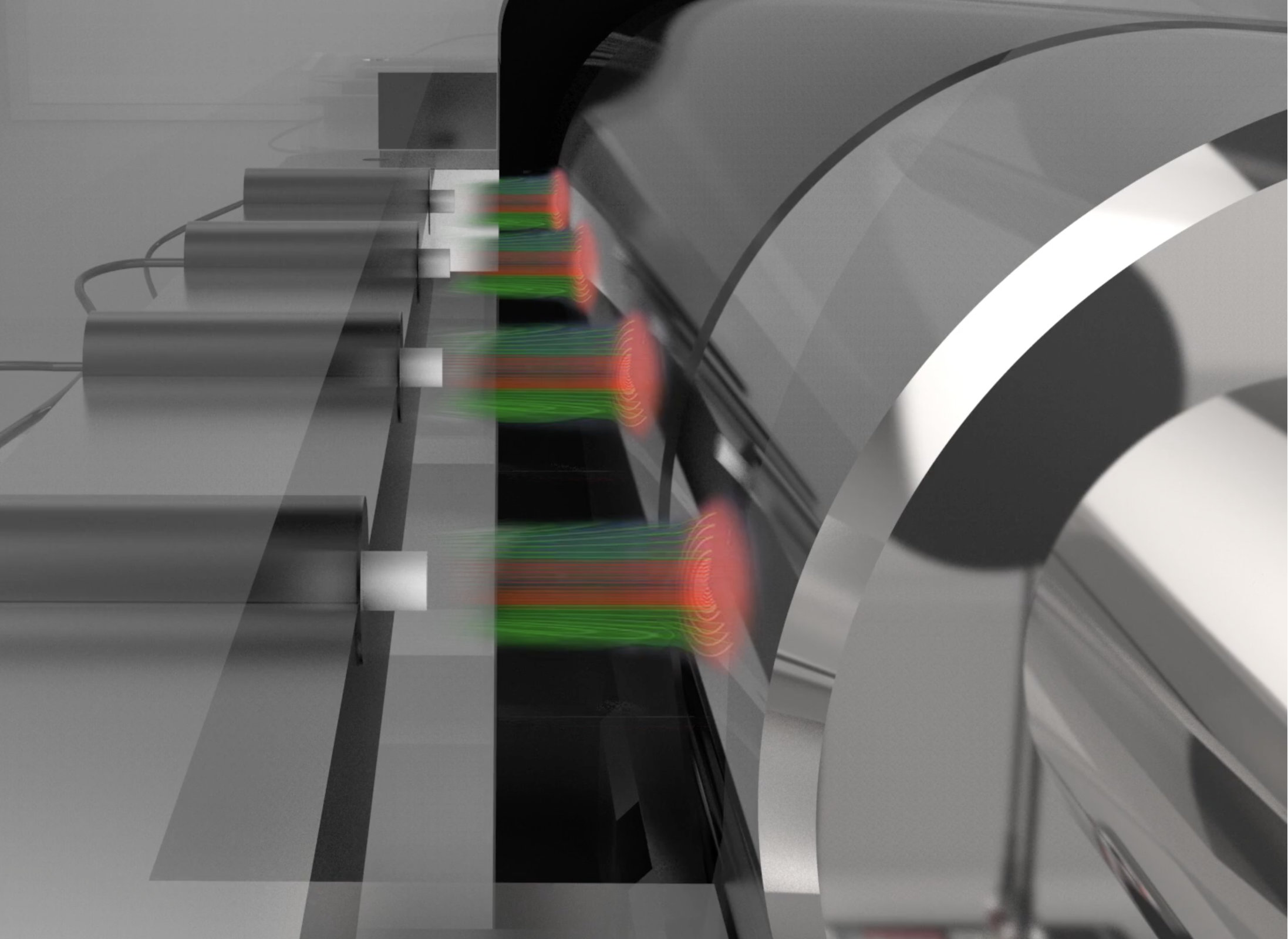
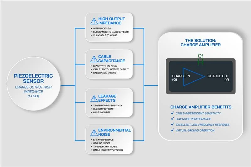
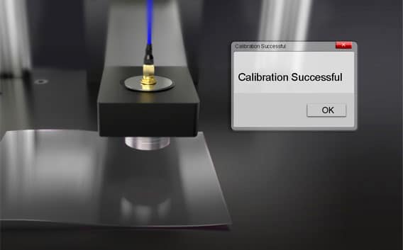
Capacitance measures the ratio of change in electric charge to the corresponding change in electrical potential (voltage). Using parallel plate technology, one plate acts as the probe, and the other as the grounded target. The capacitance between the two plates varies with the distance (gap) between them, allowing the system to measure thin film thickness with high precision. The resulting capacitance change is converted into an output voltage that is proportional to the gap, providing an accurate reading of thin film thickness at a sub-micron level.
Capacitance measurement is particularly effective for non-conductive thin films, which are typically challenging to measure using traditional methods. Unlike other methods, capacitance does not require direct contact between the probe and the target, eliminating risks such as mechanical wear, target distortion, and sample damage. Additionally, capacitance-based systems are more cost-effective than laser interferometers but offer comparable or superior performance in terms of stability and accuracy. Capacitive probes are also highly durable, performing well in strong magnetic fields and vacuum conditions, making them ideal for in-situ measurement in high-volume testing environments.
In contrast, destructive methods—such as mechanical cross-sectioning, ion beam cross-sectioning, or electron microscopy (TEM lamella preparation)—alter the sample and require extensive sample preparation, adding complexity and time to the process. These methods also do not allow for in-situ measurement, requiring microscopy and additional analysis after the process is complete.
Capacitive Thin Film Thickness Measurement Solutions

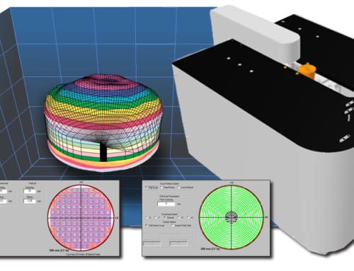
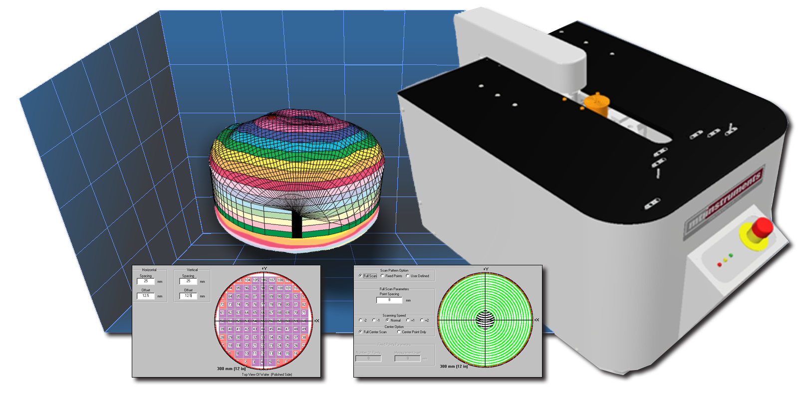
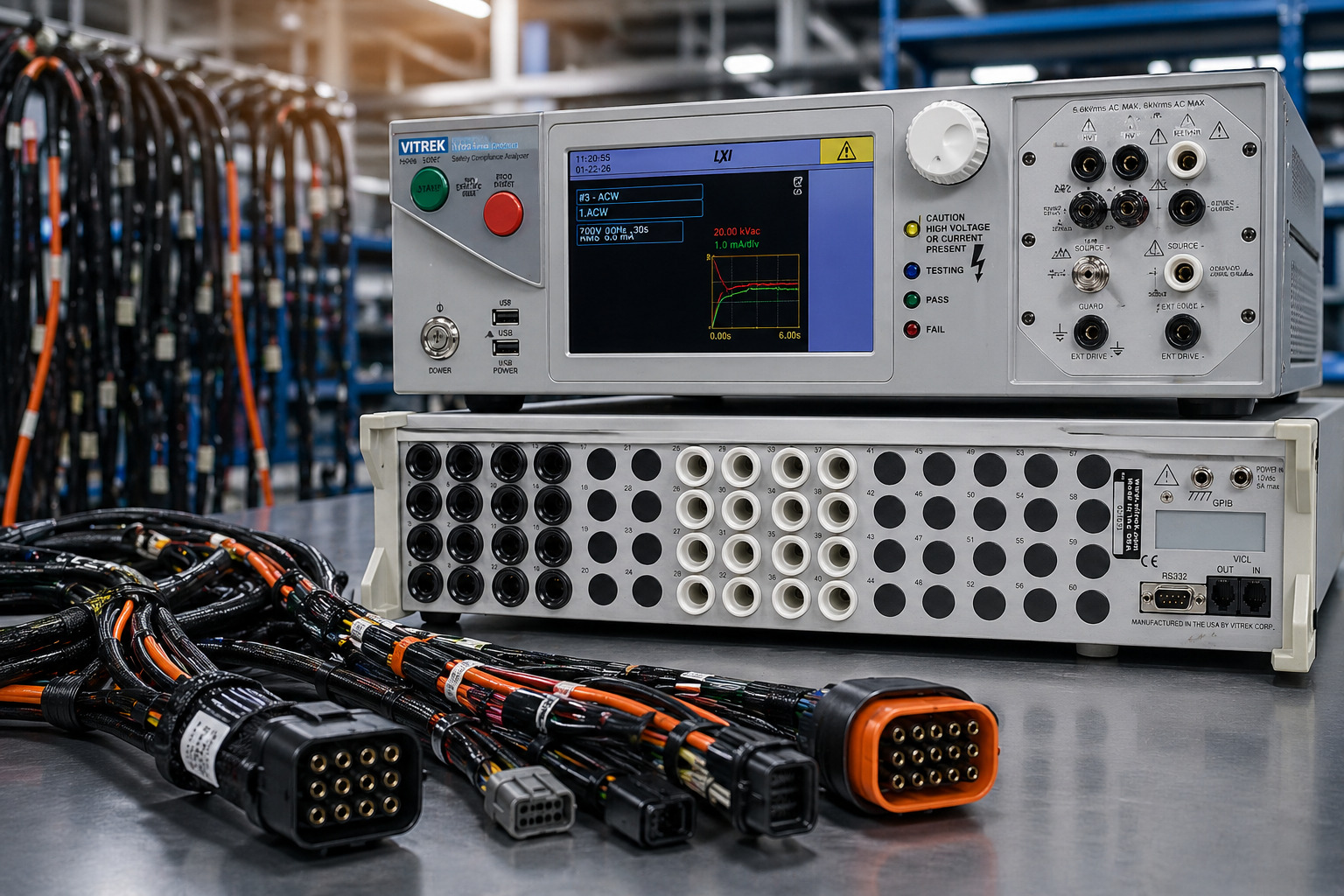
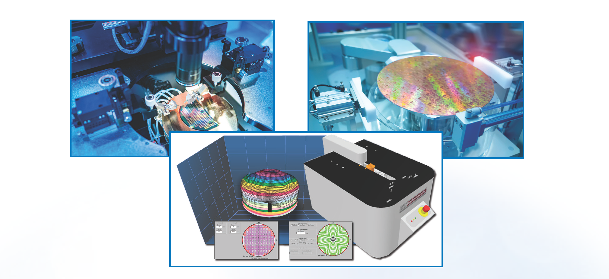
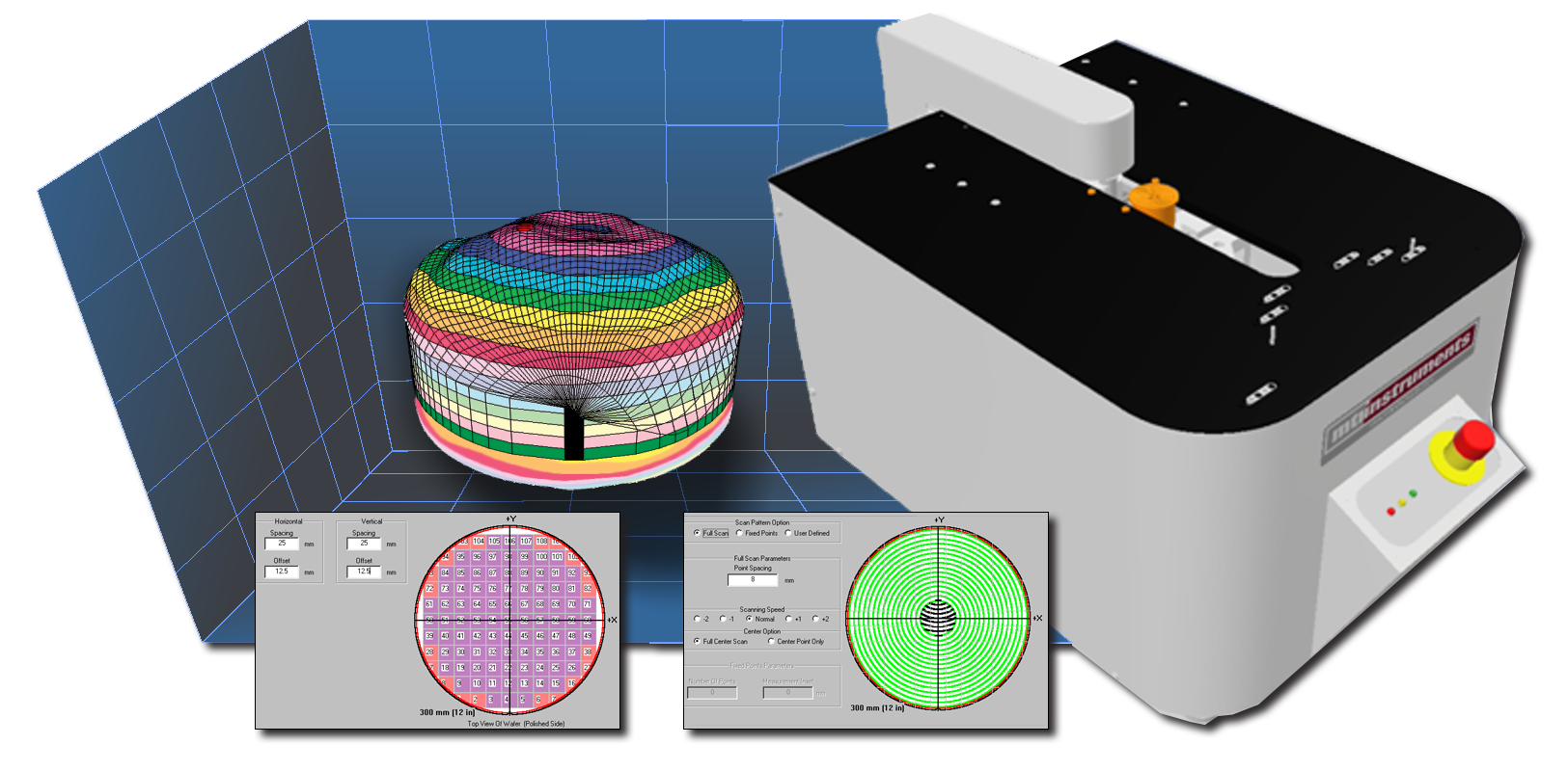
MTI Instruments offers a range of non-contact, capacitance-based solutions for accurate thin film thickness measurement. For instance, the Proforma 300iSA is a desktop, semi-automated metrology system with full surface scanning capabilities for three-dimensional wafer imaging. This system supports both conductive metallic films and non-conductive metal oxide films, offering precise thickness measurements before and after deposition. With the ability to handle wafers ranging from 3 inches to 12 inches and measuring up to 1000 µm in thickness, the Proforma 300iSA simplifies the measurement of thin films as thin as 10 µm.
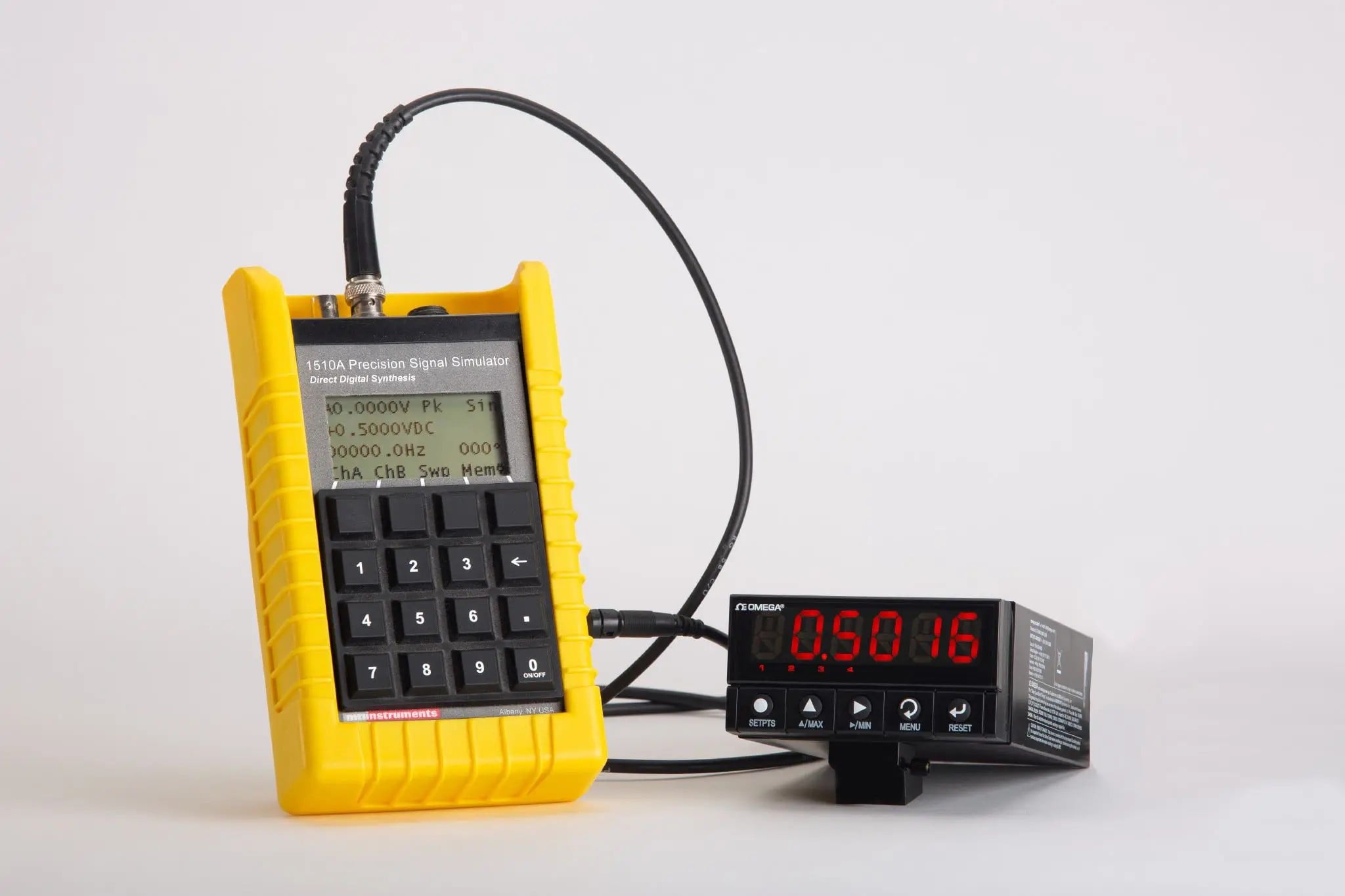
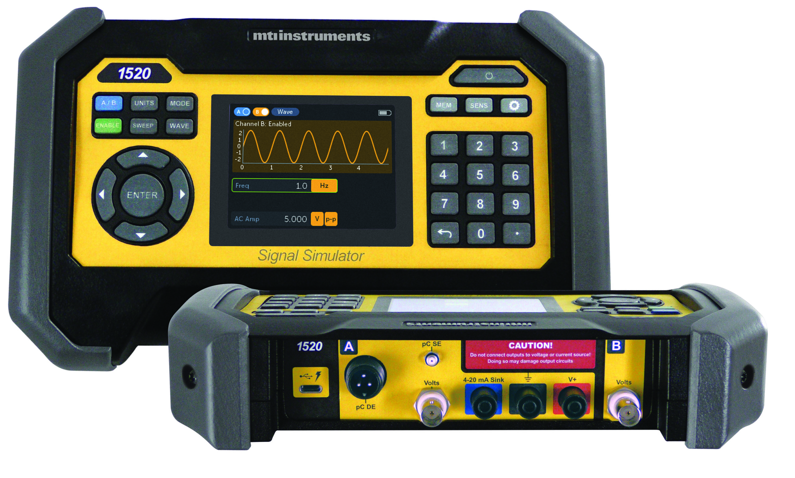
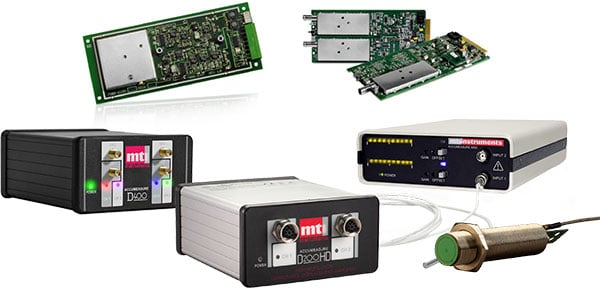
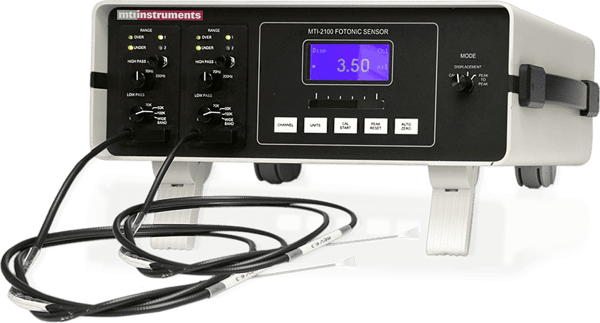
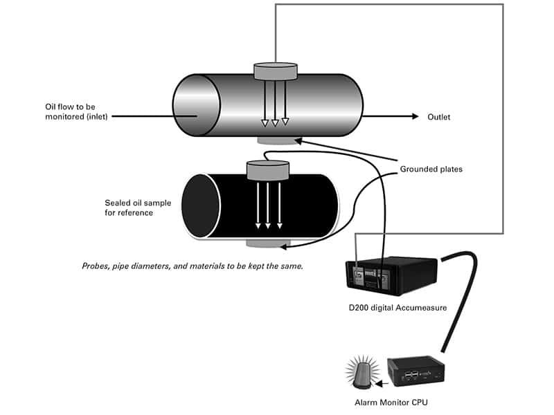
For factory floor measurements, MTI’s Accumeasure series capacitance sensors provide exceptional stability, repeatability, and accuracy. In these systems, a capacitance probe within the deposition chamber detects impedance changes as metal oxide films are deposited, allowing for real-time, in-situ thickness measurement of the dielectric material. The Accumeasure system translates the capacitance measurement into a precise 24-bit digital reading, ensuring reliable and accurate results. This technology is also applicable for measuring conductive films in real-time.
Both the Proforma 300iSA and Accumeasure systems streamline sample preparation, removing the need for destructive methods like microscopy. These instruments feature intuitive interfaces and support data export to familiar programs such as Microsoft Excel, simplifying data analysis and reporting. The Proforma 300iSA is also capable of measuring wafer thickness, thickness variation, bow, warp, and global flatness, enhancing its versatility for semiconductor applications.
Conclusion
In the semiconductor industry, precise thin film thickness measurement is critical for ensuring high-quality coatings on wafers. Capacitance-based measurement provides a non-contact, non-destructive, and highly accurate method for measuring both conductive and non-conductive coatings. MTI Instruments’ Proforma 300iSA and Accumeasure systems simplify the measurement process, reduce costs, and improve manufacturing timelines. These systems are essential for high-volume testing, providing nanometer-level accuracy and enabling in-situ measurement that traditional methods cannot achieve. For more information about MTI’s thin film thickness measurement solutions, contact us today.


