
 Aviation NewsBrief: Industry Growth Faces Trained Technician Shortage Gallery
Aviation NewsBrief: Industry Growth Faces Trained Technician Shortage
Brand-Vitrek, Industry-Aerospace, Industry-Government/Military, Industry: Transportation, Knowledge Center-GaGe, Knowledge Center-MTI, Knowledge Center-Vitrek, News-Industry
Aviation NewsBrief: Industry Growth Faces Trained Technician Shortage
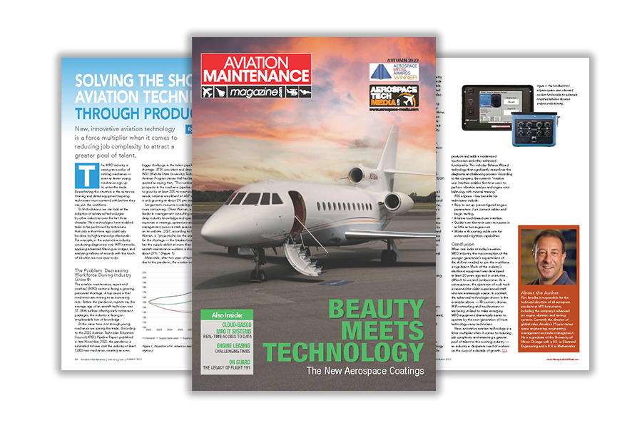
Introduction Prior to the COVID pandemic, the average age of a highly trained aircraft technician was 57. The airline industry, like so many others, reacted to the pandemic by reducing operations and offering early retirement as way of balancing the workforce with demand. Now the airline industry is experiencing unprecedented growth and thanks to the early retirement of senior MRO technicians, the industry is experiencing a shortfall in its population of qualified personnel. The Problem: Too Few Young Mechanics Joining the Ranks Not enough young mechanics are joining the trade. Exacerbating the situation is [...]

Article: Solving the Shortage of Aviation Technicians Through Product Design
he MRO industry is seeing an exodus of retiring mechanics — even as fewer young mechanics sign up to enter the trade. Exacerbating the situation is the extensive training and dated equipment aspiring technicians must contend with before they can join the workforce.
 Press Release: Vitrek Supports the Semiconductor Industry’s Urgent Demand for High-Performance Test Equipment Driven by the CHIPS and Science Act Gallery
Press Release: Vitrek Supports the Semiconductor Industry’s Urgent Demand for High-Performance Test Equipment Driven by the CHIPS and Science Act
Brand-GaGe, Brand-MTI, Brand-Vitrek, Brands-All, Industry-Manufacturing, Industry-Semiconductor, Industry-Semiconductor-Vitrek, New & Press Releases, News-All Brands, News-Events, News-GaGe, News-Industry, News-MTI, News-Vitrek, Press Releases-Vitrek
Press Release: Vitrek Supports the Semiconductor Industry’s Urgent Demand for High-Performance Test Equipment Driven by the CHIPS and Science Act
The $52.7 billion legislation passed in 2022 is driving the expansion of US-based semiconductor sector; Vitrek’s product portfolio includes test and data acquisition products essential for advanced R&D and semiconductor manufacturing.
 Video: GaGe Products for the Semiconductor Industry Gallery
Video: GaGe Products for the Semiconductor Industry
Brand-GaGe, Industry-Compliance Testing, Industry-Consumer Products, Industry-Electronics, Industry-Manufacturing, Industry-Measurement Applications, Industry-R&D, Industry-Semiconductor, Industry-Semiconductor-GaGe, Industry-Semiconductor-Videos, Knowledge Center-GaGe, News-GaGe, News-Products, News-Vitrek, Videos-GaGe
 Video: MTI Products for the Semiconductor Industry Gallery
Video: MTI Products for the Semiconductor Industry
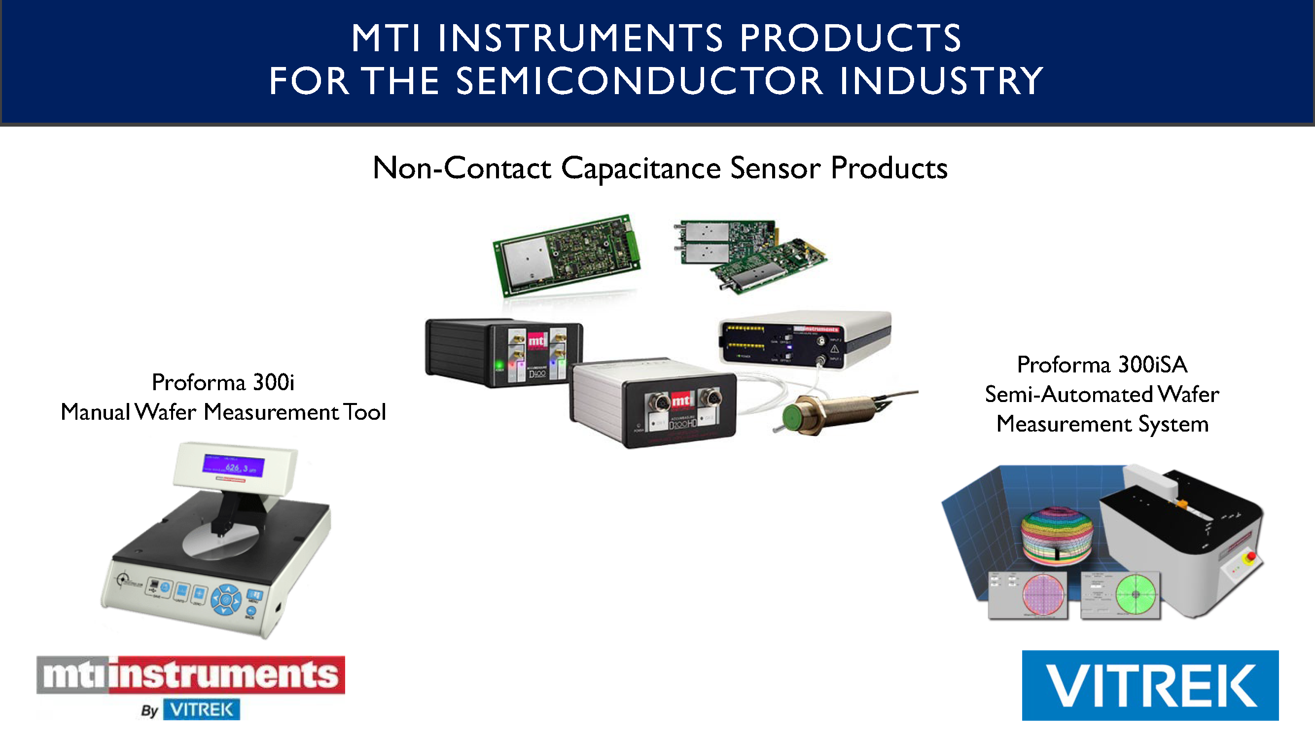
Brand-MTI, Industry-Compliance Testing, Industry-Consumer Products, Industry-Electronics, Industry-Manufacturing, Industry-Measurement Applications, Industry-R&D, Industry-Semiconductor, Industry-Semiconductor-MTI, Industry-Semiconductor-Videos, Knowledge Center-MTI, News-MTI, Videos-MTI, Videos-MTI-Capacitance Sensors, Videos-MTI-Manual Semiconductor Metrology System, Videos-MTI-Semiautomated Metrology System
 MTI Instruments Whitepaper: Capacitance Guide for Industrial Applications Gallery
MTI Instruments Whitepaper: Capacitance Guide for Industrial Applications
Brand-MTI, Industry-Aerospace, Industry-Automotive, Industry-Battery, Industry-Compliance Testing, Industry-Consumer Products, Industry-Electronics, Industry-Energy, Industry-Government/Military, Industry-Industrial Processing, Industry-Lighting, Industry-Manufacturing, Industry-Measurement Applications, Industry-OEM, Industry-R&D, Industry-Semiconductor, Industry-Semiconductor-MTI, Industry-Sensors, Industry: Transportation, Knowledge Center-MTI, News-MTI, Whitepapers-MTI
MTI Instruments Whitepaper: Capacitance Guide for Industrial Applications
Capacitance Guide for Industrial Applications This guide from MTI Instruments explains what you need to know about using electrical capacitance for measurement in industrial applications, including advanced manufacturing. Basic Principles Capacitance is the ratio of the change in an electric charge to the corresponding change in its electrical potential (i.e., voltage). Capacitors, components that that have the “capacity” to store an electric charge, consist of conductive parallel plates that don’t touch or connect with each other. Instead, these metal plates are electrically-separated by air or a layer of insulating material (i.e., the dielectric). MTI’s [...]
 Whitepaper: Why Capacitance? Benefits and Applications of Digital Capacitive Sensors Gallery
Whitepaper: Why Capacitance? Benefits and Applications of Digital Capacitive Sensors
Brand-MTI, Industry-Automotive, Industry-Compliance Testing, Industry-Consumer Products, Industry-Electronics, Industry-Industrial Processing, Industry-Manufacturing, Industry-Measurement Applications, Industry-Semiconductor, Industry-Semiconductor-MTI, Industry-Sensors, Knowledge Center-MTI, News-MTI, News-Vitrek, Whitepapers-MTI
Whitepaper: Why Capacitance? Benefits and Applications of Digital Capacitive Sensors
Industry applications illustrate the versatility and benefits of today's digital capacitive sensor technology. The electrical capacitance formed between a capacitance probe and target surface varies as a function of the distance, or gap, between those two surfaces.
Ultrasonic Tissue Characterization
Ultrasonic Tissue Characterization Customer Case This customer's application is Ultrasonic Tissue Characterization. Their ultrasonic sensors transmit 16 signals. The customer's requirement is to capture 512 points on the 16 channels, average them together, and then store the data in a buffer, with the system running continuously. They would like to be able to update the average buffer and recapture data as fast as possible. They would then like to log the data to disk or process the data and display an image on the screen. Since the signals coming in from their ultrasonic sensors are very weak, the customer [...]
 Whitepaper: Semiconductor Wafer Measurement for Increased Productivity Gallery
Whitepaper: Semiconductor Wafer Measurement for Increased Productivity
Brand-GaGe, Brand-MTI, Brand-Vitrek, Brands-All, Industry-Consumer Products, Industry-Electronics, Industry-Manufacturing, Industry-OEM, Industry-Semiconductor, Industry-Semiconductor-MTI, Knowledge Center-MTI, News-Industry, News-MTI, Whitepapers-MTI
Whitepaper: Semiconductor Wafer Measurement for Increased Productivity
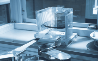
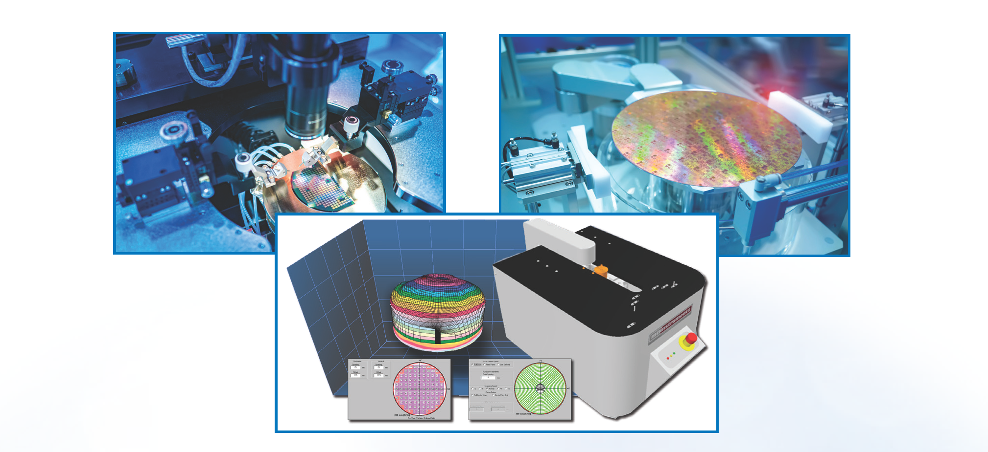
Semiconductor Wafer Measurement for Increased Productivity This three-part article describes how manufacturers leverage capacitance-based inspection systems for semiconductor wafers. The article reviews best-practices, consequences of failing to inspect semiconductor wafers and benefits of using semi-automated, fully-automated and manual systems for wafer metrology and inspection. Part 1: Why Disc Geometry Matters in Wafer Production Semiconductor wafers are cut from cylindrical silicon crystals, or ingots. The flatness of these disc-shaped wafers is controlled to tight tolerances to ensure that the entire wafer surface is suitable for integrated circuit (IC) production. If disc geometry is out-of-spec [...]





The Cost of Failing to Inspect Semiconductor Wafers
This is the second of three articles in Semiconductor Wafer Measurement for Increased Profitability. The first article in this series explains why disc geometry matters. The third article describes the benefits of using semi-automated, fully-automated, and manual systems for wafer metrology and inspection. Most semiconductor wafers are made of silicon, the second most common element in the Earth’s crust. Yet, silicon’s abundance does not mean that wafers are inexpensive. The pure form of silicon that’s used in semiconductors does not occur naturally and must be refined and mixed with a dopant that alters material properties and electrical characteristics. Silicon ingots are formed, wafers [...]