
MTI Video: Wafer Inspection & Metrology Startup (Proforma 300iSA)
https://youtu.be/mawagL6Yg3U
MTI Video: Wafer Inspection and Metrology Tutorial (Proforma 300i)
https://www.youtube.com/watch?v=nGkbpG2sz_k Learn More Download this brochure to learn more about the Proforma 300i wafer measurement system for semiconducting and semi-insulating wafers. This article in AZO Sensors also provides information.
New Video from MTI! Closed-loop System to Monitor and Control Conductive Film Thickness During Manufacturing
Closed-loop System to Monitor and Control Conductive Film Thickness During Manufacturing This animation demonstrates how Accumeasure with capacitance probes can be used as a solution to measure and control conductive film thickness in a production line where these measurements can be fed back to a controller which adjusts the roller(s) to increase or decrease the gap to keep the film’s thickness within specification. The MTI Instruments Capacitive system has greater than 100 nm resolution and 1um accuracy. This solution is appropriate for measuring the following: EV battery plate thickness Non-woven conductive material thickness Conductive film thickness Roll-to-roll conductive [...]
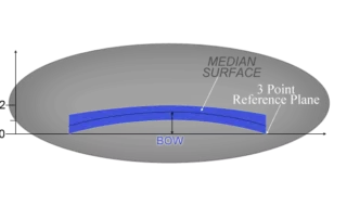
WAFER MEASUREMENT – UNGROUNDED
Industry Semiconductor Applications Wafer Measurement – Ungrounded Measurement Type Metrology Description MTI Instruments Inc. has developed a thickness measurement device that eliminates the effect of varying target conductivity. Called the Push-Pull probe, it’s a unique version of the AccumeasureTM amplifier series. This special design provides accurate surface information for wafer bow and warp. Bow is the deviation of the center point of the median surface of a free, un-clamped wafer from the median surface to the reference plane. Where, the reference plane is defined by three corners of equilateral triangle. This [...]
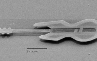


PHOTOLITHOGRAPHY USING CAPACITANCE SENSORS
Industry Semiconductor Applications Lithography Optics Position Focus Measurement Type Positioning Description When it comes to photolithography, how accurate are our sensors? Photo by D. Carr and H. Craighead, Cornell - The world’s smallest guitar is 10 micrometers long — about the size of a single cell — with six strings each about 50 nanometers, or 100 atoms, wide. Made by Cornell University researchers from crystalline silicon, it demonstrates a new technology for a new generation of electromechanical devices. Even the world’s smallest guitar’s 2 micron [...]
 Creating a Compensation File for a Recipe for the Proforma 300iSA – Video Gallery
Creating a Compensation File for a Recipe for the Proforma 300iSA – Video
Brand-MTI, Industry-Compliance Testing, Industry-Electronics, Industry-Manufacturing, Industry-Semiconductor, Industry-Semiconductor-MTI, Industry-Semiconductor-Videos, News-MTI-Metrology, Products-MTI-Semiconductor/Metrology, Videos-MTI-Manual Semiconductor Metrology System, Videos-MTI-Semiautomated Metrology System, z1
 The Benefits of Manual, Semi-Automated, and Fully-Automated Systems for Semiconductor Wafer Inspection and Metrology Gallery
The Benefits of Manual, Semi-Automated, and Fully-Automated Systems for Semiconductor Wafer Inspection and Metrology
Application Notes-MTI, Brand-MTI, Industry-Consumer Products, Industry-Electronics, Industry-Manufacturing, Industry-Semiconductor, Industry-Semiconductor-MTI, News-MTI-Metrology, Products-MTI-Semiconductor/Metrology, z1
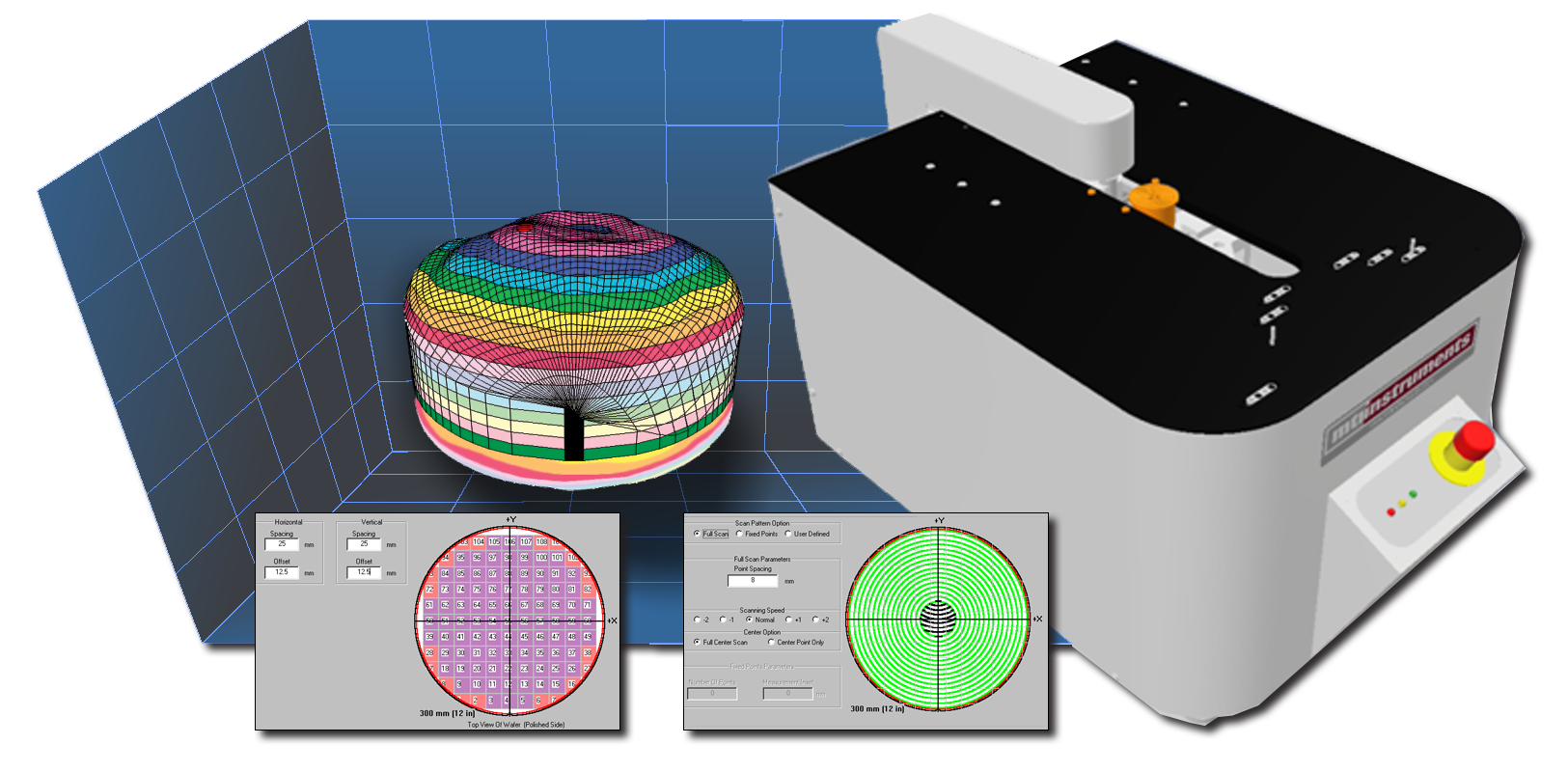
The Benefits of Manual, Semi-Automated, and Fully-Automated Systems for Semiconductor Wafer Inspection and Metrology
This is the third of three articles in Semiconductor Wafer Measurement for Increased Profitability. The first article in this series explains why disc geometry matters. The second article examines the cost of failing to inspect semiconductor wafers. Fully automated systems that can load, scan, and unload wafers are fast, convenient, and efficient at high volumes. They’re useful for checking every wafer in every batch, but these systems are expensive. Semi-automated and manual systems cost significantly less and are generally used for lower volumes; however, they’re also easy-to-use and can make fast, accurate measurements that support production flow. Semi-automated and [...]