
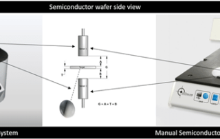
 Why Disc Geometry Matters In Wafer Production Gallery
Why Disc Geometry Matters In Wafer Production
Application Notes-MTI, Brand-MTI, Industry-Consumer Products, Industry-Electronics, Industry-Manufacturing, Industry-Semiconductor, Industry-Semiconductor-MTI, News-MTI-Metrology, Products-MTI-Semiconductor/Metrology, z1
Why Disc Geometry Matters In Wafer Production
This is the first of three articles in Semiconductor Wafer Measurement for Increased Profitability. The second article examines the cost of failing to inspect semiconductor wafers. The third article describes the benefits of using semi-automated, fully-automated, and manual systems for wafer metrology and inspection. Semiconductor wafers are cut from cylindrical silicon crystals, or ingots. The flatness of these disc-shaped wafers is controlled to tight tolerances to ensure that the entire wafer surface is suitable for integrated circuit (IC) production. If disc geometry is out-of-spec after cutting, it may be possible to reprocess the wafer. Cutting is only the first [...]

Measuring Glass wafer thickness with a Proforma 300i
Measuring glass substrate thickness with a Proforma 300i Semiconductor Glass Wafer Thickness Measurement Thickness Applications testing of glass (substrate) thickness An applications experiment was made with the MTI Proforma 300i Semiconductor thickness system to determine if it’s useful to measure glass substrate thicknesses typically found as support structures for Si semiconductors that are used for fabricating MEMs components and other thin Si wafers. The MEMs Silicon wafer is so thin after grinding that it needs the support of a thicker substrate to prevent breakage of the wafer during the back grinding/thinning [...]
 Advantages of Measuring Semiconductor Thin Film Thickness with Capacitance Gallery
Advantages of Measuring Semiconductor Thin Film Thickness with Capacitance
Application Notes-MTI, Brand-MTI, Industry-Compliance Testing, Industry-Electronics, Industry-Manufacturing, Industry-R&D, Industry-Semiconductor, Industry-Semiconductor-MTI, Industry-Sensors, Products-MTI-Capacitance, Products-MTI-Laser/Fiber Optic, Products-MTI-Semiconductor/Metrology, Z-REPUB, z1
Advantages of Measuring Semiconductor Thin Film Thickness with Capacitance
Thin Film Thickness Measurement Using Capacitance in the Semiconductor Industry In the semiconductor industry, the precise measurement of thin film thickness is crucial for ensuring the quality and functionality of wafer coatings. Thin films are deposited onto silicon and other wafer materials one atomic layer at a time, and the thickness of these coatings significantly impacts the wafer’s electrical, optical, and mechanical properties. Thin film thickness measurement is particularly important for semiconductor wafers, which may have either conductive metallic films or non-conductive metal oxide films deposited onto them. Common deposition methods include chemical vapor deposition (CVD) and physical vapor [...]
 Contact vs. Non-Contact Measurement and Linear Displacement Sensors Gallery
Contact vs. Non-Contact Measurement and Linear Displacement Sensors
Application Notes-MTI, Brand-MTI, Industry-Compliance Testing, Industry-Consumer Products, Industry-Electronics, Industry-Manufacturing, Industry-Semiconductor, Industry-Semiconductor-MTI, Industry-Sensors, Products-MTI-Capacitance, Z-REPUB, z1, ZOK
Contact vs. Non-Contact Measurement and Linear Displacement Sensors
Contact vs. Non-Contact Measurements Choosing between a contact measurement system and a non-contact measurement system requires careful evaluation of your application’s performance needs, material properties, environmental conditions, and measurement goals. Each system type offers unique advantages- and understanding these distinctions can help you make a more informed decision. Let's explores how contact and non-contact measurement techniques work, their strengths and limitations, and where they’re best applied. What Are Contact Measurement Systems? Contact measurement systems involve tools and sensors that physically touch the object to determine various physical characteristics. These systems are widely used in dimensional metrology, offering high precision, [...]


Semiconductor Wafer Lapping and Displacement Measurement
Semiconductor Wafer Lapping and Displacement Measurement Semiconductor Semiconductor Wafer Manufacturing Displacement Description Semiconductor Wafer Lapping and Displacement Measurement This application note explains how MTI’s Accumeasure technology was used with a lapping machine to measure displacement (wafer material removal) and determine the new semiconductor wafer thickness. Changes in electrical capacitance (displacement) were measured and then directly converted into a 24-bit digital reading to obtain precise digital thickness measurements. During lapping, a wafer of known start thickness is placed on a rotary lapping table. The backside of the wafer faces downward and toward [...]
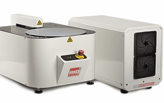 Why Demand for SiC Wafers is Soaring and Durable Gallery
Why Demand for SiC Wafers is Soaring and Durable
Brand-MTI, Industry-Consumer Products, Industry-Electronics, Industry-Manufacturing, Industry-Semiconductor, Industry-Semiconductor-MTI, MTI Blog, News-MTI, News-MTI-Metrology, Products-MTI-Semiconductor/Metrology, Z-REPUB, z1

Why Demand for SiC Wafers is Soaring and Durable
Silicon carbide (SiC) wafers are in high demand, particularly in high-temperature applications. Silicon carbide (SiC), a semiconductor material made of both silicon and carbon, can withstand extreme temperatures of up to 2700°C. Often referred to as carborundum, SiC’s unique properties also make it a key material in non-electronic applications such as bulletproof vests, extrusion dies, sandpaper, and high-performance disc brakes. In the electronics industry, SiC wafers are crucial for devices operating under high temperatures, high voltages, or both. For example, they are used in electric vehicle (EV) power electronics, 5G communication systems, and LED technology, making SiC a material [...]
Wafer Stress Analysis Using the 300iSA
Wafer Stress Analysis Using MTI Instruments Proforma 300iSA Wafer processing involves several stages that can lead to mechanical changes in the wafer structure. These changes, or stresses, may result in deformities, making the wafer either unusable or only marginally usable. To evaluate these stresses and determine the wafer's quality, wafer stress measurement is essential. The Proforma 300iSA wafer characterization tool offers a powerful solution for wafer stress analysis. It allows for the analysis of a wafer both before and after processing. By comparing these two states, the Proforma 300iSA effectively evaluates the wafer's stress levels and mechanical alterations, providing [...]
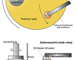 CMP and Capacitance-Based Semiconductor Wafer Measurement Gallery
CMP and Capacitance-Based Semiconductor Wafer Measurement
Application Notes-MTI, Brand-MTI, Industry-Compliance Testing, Industry-Consumer Products, Industry-Electronics, Industry-Manufacturing, Industry-Semiconductor, Industry-Semiconductor-MTI, Industry-Sensors, Products-MTI-Capacitance, Products-MTI-Semiconductor/Metrology, z1

CMP and Capacitance-Based Semiconductor Wafer Measurement
Chemical mechanical polishing (CMP) uses chemical oxidation and mechanical abrasion to selectively remove material from semiconductor wafers in order to achieve very high levels of planarity. The planarity, or flatness, of these wafers is important for optical lithography, a microfabrication technique that produces integrated circuits (ICs) by transferring a geometric pattern from a photomask to a light-sensitive chemical photoresist. Also known as photolithography or UV lithography, optical lithography can produce a geometric pattern on a thin film or directly onto the substrate. Semiconductor Wafer Measurements: Flatness and Shape During optical lithography, variations in wafer flatness must be smaller than [...]
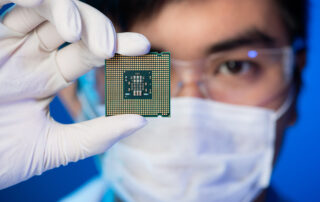 MEMS and Capacitance-Based Semiconductor Wafer Measurement Gallery
MEMS and Capacitance-Based Semiconductor Wafer Measurement
Application Notes-MTI, Brand-MTI, Industry-Compliance Testing, Industry-Consumer Products, Industry-Electronics, Industry-Manufacturing, Industry-Semiconductor, Industry-Semiconductor-MTI, Industry-Sensors, Products-MTI-Capacitance, Products-MTI-Semiconductor/Metrology, Z-REPUB, z1

MEMS and Capacitance-Based Semiconductor Wafer Measurement
MEMS Technology and Capacitance-Based Wafer Measurement Micro-electrical-mechanical systems (MEMS) are tiny devices that house electrical and mechanical components on a single silicon chip or integrated circuit (IC). They integrate mechanical structures with electronics that are normally fabricated with complementary metal-oxide-semiconductor (CMOS) technologies. In addition to miniaturization, the benefits of MEMS include expanded functionalities at lower cost and with improved performance and reliability. With MEMS devices, critical physical dimensions range from smaller than one micron (µ) to larger than several millimeters (mm). In complex systems, multiple moving elements may be controlled by integrated electronics. Examples of the mechanical components in [...]
 Wafer Backgrinding and Semiconductor Thickness Measurements Gallery
Wafer Backgrinding and Semiconductor Thickness Measurements
Application Notes-MTI, Brand-MTI, Industry-Compliance Testing, Industry-Consumer Products, Industry-Electronics, Industry-Manufacturing, Industry-Semiconductor, Industry-Semiconductor-MTI, News-MTI-Instrumentation, News-MTI-Metrology, Products-MTI-Capacitance, Products-MTI-Semiconductor/Metrology, Z-REPUB, z1
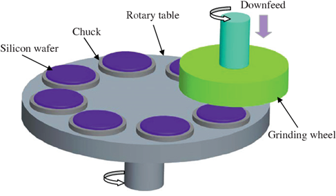
Wafer Backgrinding and Semiconductor Thickness Measurements
Wafer Backgrinding and Thickness Measurements in Semiconductor Manufacturing Wafer backgrinding, also known as wafer thinning or wafer lapping, is a critical step in semiconductor packaging. This process, which involves grinding the backside of a semiconductor wafer, reduces its thickness to enable the stacking of integrated circuits (ICs) and support high-density packaging. The thickness of the wafer plays a crucial role in determining the overall size of the package, an important factor as modern electronics such as smartphones, laptops, and other devices continue to get thinner and more compact. In applications like MEMS (Micro-Electro-Mechanical Systems), the backgrinding process also affects [...]