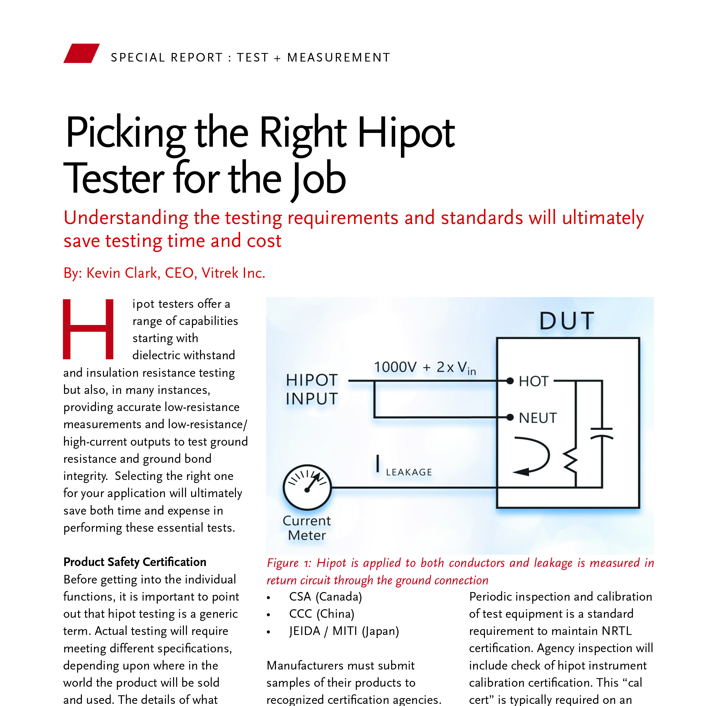
This is the first of three articles in Semiconductor Wafer Measurement for Increased Profitability. The second article examines the cost of failing to inspect semiconductor wafers. The third article describes the benefits of using semi-automated, fully-automated, and manual systems for wafer metrology and inspection.
Semiconductor wafers are cut from cylindrical silicon crystals, or ingots. The flatness of these disc-shaped wafers is controlled to tight tolerances to ensure that the entire wafer surface is suitable for integrated circuit (IC) production. If disc geometry is out-of-spec after cutting, it may be possible to reprocess the wafer. Cutting is only the first step in wafer processing, however, and subsequent steps such as lapping and polishing, thin film deposition, and lithography can add costs that result in significant waste if a wafer fails to meet dimensional specifications. This article, the first in a series, explains why disc geometry matters at each step in wafer processing – and what can go wrong.
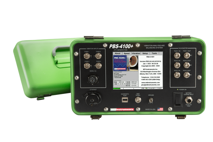
MTI Instruments makes capacitance-based inspection and metrology systems for semiconductor wafers. In the front end of the wafer processing procedure, these systems can measure disc geometry and thereby ensure that wafers, which are often valued at thousands of dollars, are suitable for additional operations. MTI’s Proforma family of products, and Digital Accumeasure technology, provide inspection and measurement solutions that are fast, easy-to-use, and cost-effective. For the semiconductor industry, the benefits of using these systems include increased profitability through reduced waste and costs.

Wafer Cutting
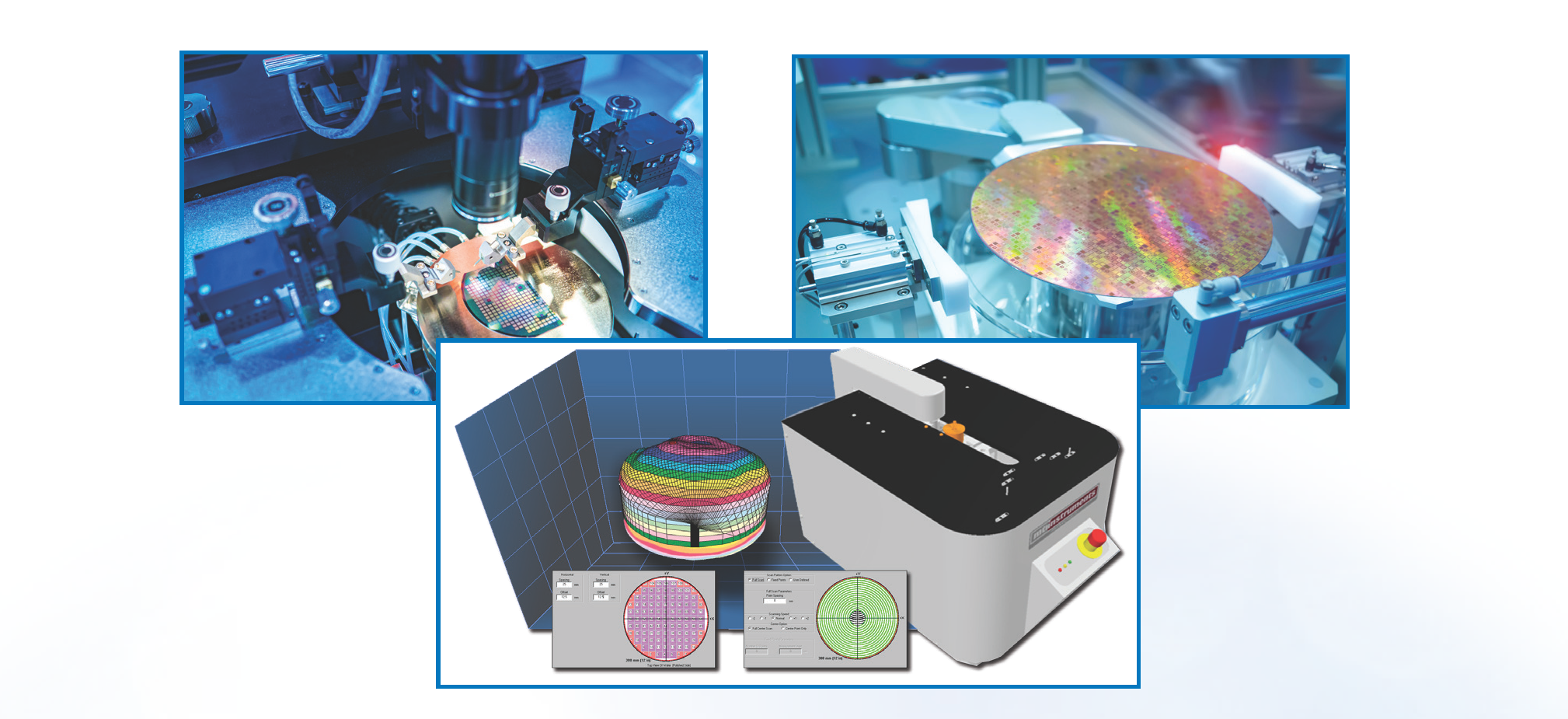
During wafer sawing, silicon ingots are sliced to a specific thickness. The diameter of a slice determines the diameter (e.g., 300 mm), which is typically referred to as the “size”, of the wafer. To avoid ruining the disc and creating scrap (or requiring reprocessing), wafer cutters need to use the right type of wire saw based on the thickness of the disc and the width of the “streets”, or cut lines, that separate individual dies. It’s also important to minimize heat buildups that can result in chipping or cracking, or the production of excessive dust.
There are many types of wire saws, including ones that are manual or automated, support single-wire or multi-wire cutting, cut in one or two directions, and are mounted on different sized hubs with varying spindle rotational speeds. Through proper tool selection and parameter optimization, wafer cutters can ensure that a disc’s geometry is suitable for additional processing. MTI’s Proforma 300i manual metrology system is a wafer thickness gauge and differential measurement system that provides a cost-effective alternative to full-automated systems. The Proforma 300iSA can also be used.
Lapping and Polishing

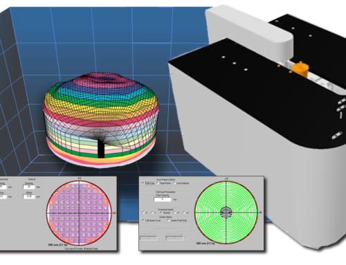
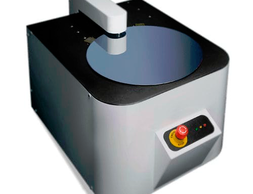
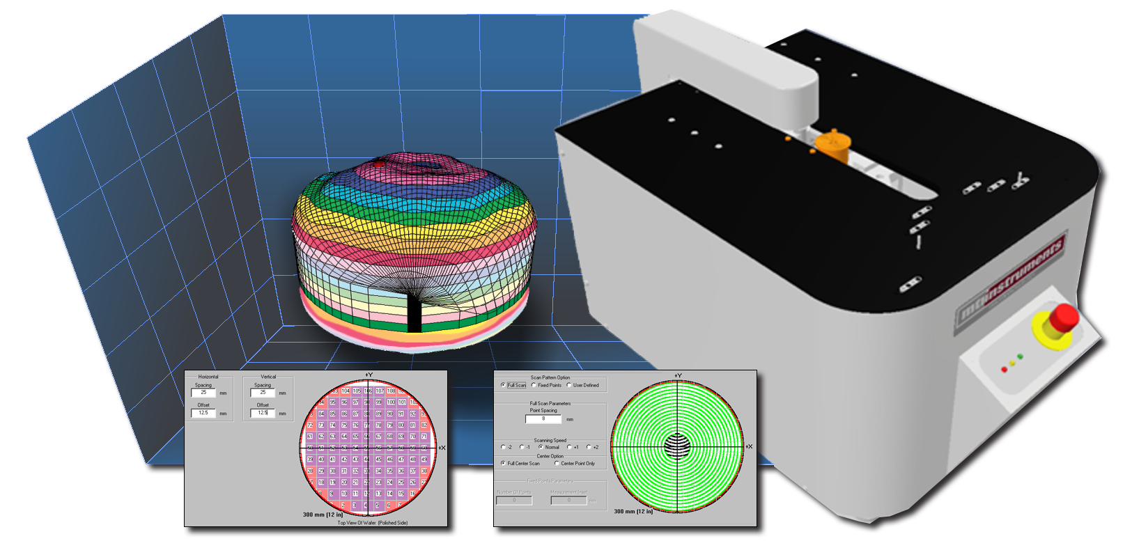
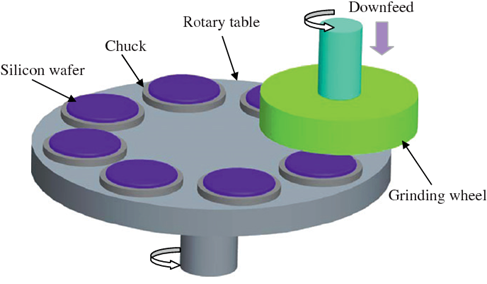
Figure 1: Rotary table for semiconductor wafer lapping
Semiconductor lapping is a mechanical process in which a pad with an abrasive liquid is used to remove excess material from a wafer substrate. During lapping, a wafer of a known thickness is placed on a rotary lapping table. The front side of the wafer faces downward and toward a lapping surface that rotates and removes unwanted material. The amount of material that is removed varies by device type, and the entire process needs to be tightly controlled to avoid removing too much or too little material. Measuring wafer thickness and total thickness variation (TTV) supports process control for proper material removal.
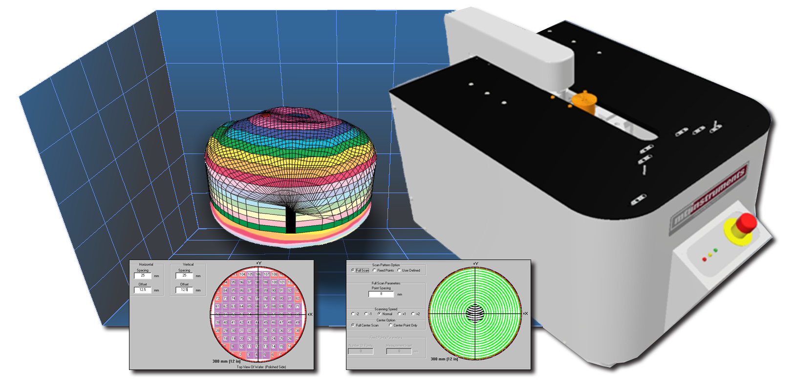
Polishing produces thinner discs, eliminates subsurface damage, and creates stronger and more flexible wafers. Many polishing methods require considerable operator skill, however. They can also be difficult to replicate since abrasion needs to be even across the wafer. Without a precise, consistent, and close-tolerance cut-rate, inspection may reveal insufficient flatness and an out-of-spec geometry. MTI’s Proforma 300iSA semi-automated metrology system provides full surface scanning and delivers a robust set of measurements that includes bow and warp. Like the Proforma 300i, it also costs less than fully automated wafer inspection and metrology systems.
Thin Film Deposition
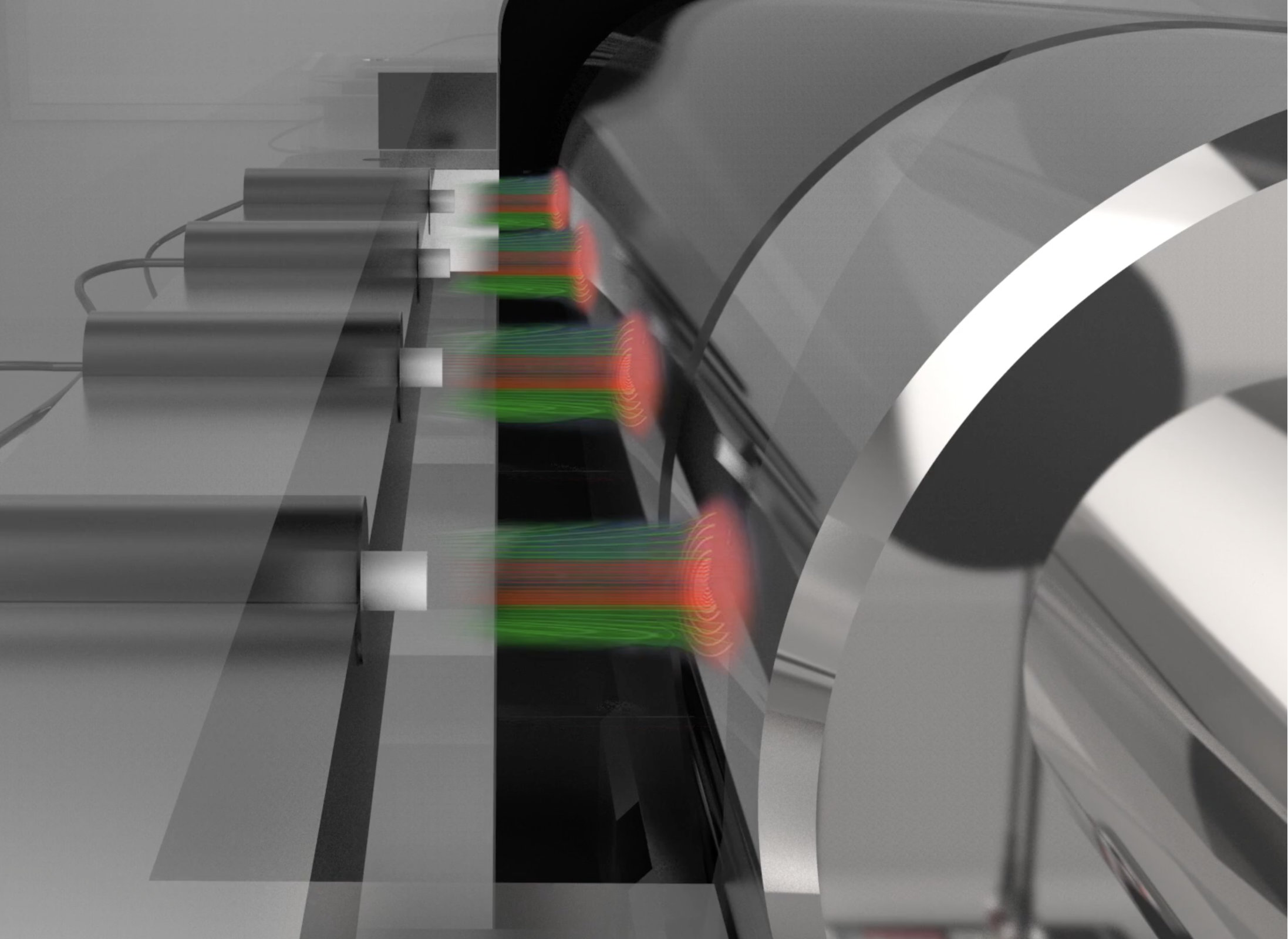
Thin films are deposited onto wafers to impart electrical, optical, and mechanical properties that enhance semiconductor performance; however, these coatings need to have a specific thickness that is uniform across the entire wafer substrate. Irregular deposition that is too thin (or too thick) in spots may not meet performance requirements and, consequently, can result in wafer waste. Whether the deposition method is chemical or physical, it is important to measure a wafer’s thickness both before and after thin film deposition.
MTI’s capacitance-based systems provide a high level of stability, repeatability, and accuracy during inspection and measurement. For example, during the build-up of a metal oxide film, a consumable capacitance probe within the deposition chamber can measure the thickness of the dielectric material by detecting the impedance change and using a co-located ground electrode. With MTI’s Digital Accumeasure, an amplifier located outside of the chamber can convert a highly precise capacitive electric field into a highly precise 24-bit digital deposition thickness reading. This technology can also be used to measure the thickness of conductive films through pre-deposition and post-deposition thickness measurements.
Lithography
Semiconductor lithography creates ICs by transferring complex patterns of geometric shapes onto thin films. With optical lithography, or photolithography, variations in the wafer surface need to be smaller than the depth of focus of the exposure tools. Because previous wafer processing steps such as grinding, lapping and polishing can impact disc geometry, it is important to measure thickness, TTV, warp, and bow. Otherwise, the expensive manufacturing equipment that is used in semiconductor lithography can add costs that result in significant waste.
The reticle, or photomask, in optical lithography is the master template for an IC design. If the reticle is not co-planar with the wafer, poor exposure and defective ICs may result. Traditionally, lithography companies used capacitance probes to keep the reticle co-planar with the wafer; however, optical sensors are now used instead because they can achieve a larger standoff distance. If stand-off is not an issue, capacitance still provides a fast, cost-effective, and relatively easy-to-use measurement technology. MTI’s capacitance probes are stable, precise, and capable of nanometer resolution.
Wafer Inspections and Technology Comparisons
MTI Instruments’ capacitance-based metrology and inspection systems enable the semiconductor industry to inspect wafers up to the lithography process and, therefore, avoid manufacturing waste. As the next article in this series explains, failure to inspect wafers at each step of the process can carry significant costs. The third and final article in this series compares fully automatic, semi-automatic, and manual inspection and metrology systems and provides a closer look at MTI’s Proforma 300i and 300iSA products.

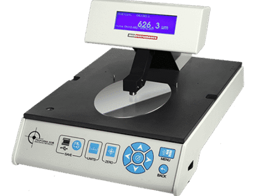
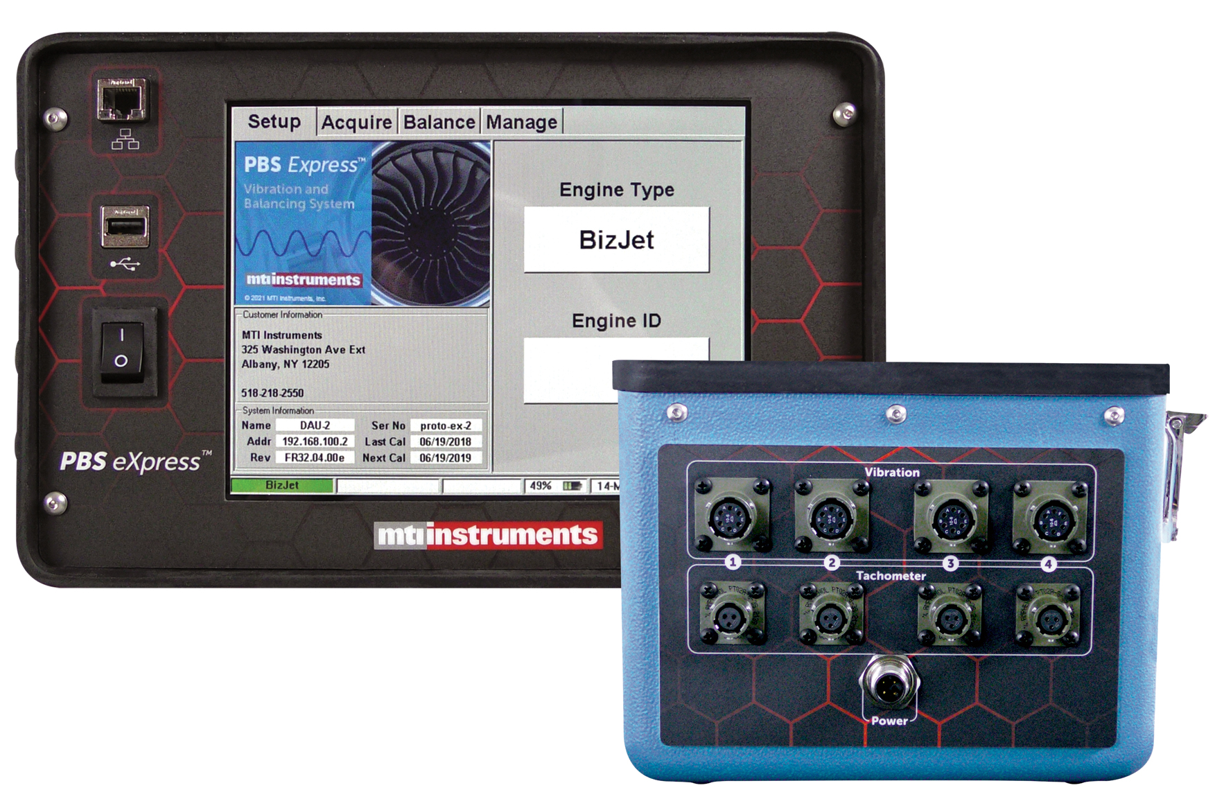
MTI Semi-Automated Proforma 300iSA Thickness Metrology Tool (Left)


