This is the third of three articles in Semiconductor Wafer Measurement for Increased Profitability. The first article in this series explains why disc geometry matters. The second article examines the cost of failing to inspect semiconductor wafers.
Fully automated systems that can load, scan, and unload wafers are fast, convenient, and efficient at high volumes. They’re useful for checking every wafer in every batch, but these systems are expensive. Semi-automated and manual systems cost significantly less and are generally used for lower volumes; however, they’re also easy-to-use and can make fast, accurate measurements that support production flow. Semi-automated and manual systems also support spot testing, or wafer sampling, in a batch.
Within the semiconductor industry, there are applications for each type of system. For example, fully automated systems may be required for inspecting and measuring critical, high-value central processing units (CPUs) where a manufacturer wants to check every wafer. For less complex microelectronics, or for less valuable integrated circuits (ICs), a manufacturer may decide that it’s more cost-effective to sample representative wafers instead. There are also ICs, or discrete components, where line widths are large and the maximum focal plane deviation, a measure of flatness, is less critical. With applications like these, a manual or semi-automated system can provide a cost-effective solution.
Proforma Technology for Non-Contact Wafer Inspection
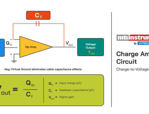
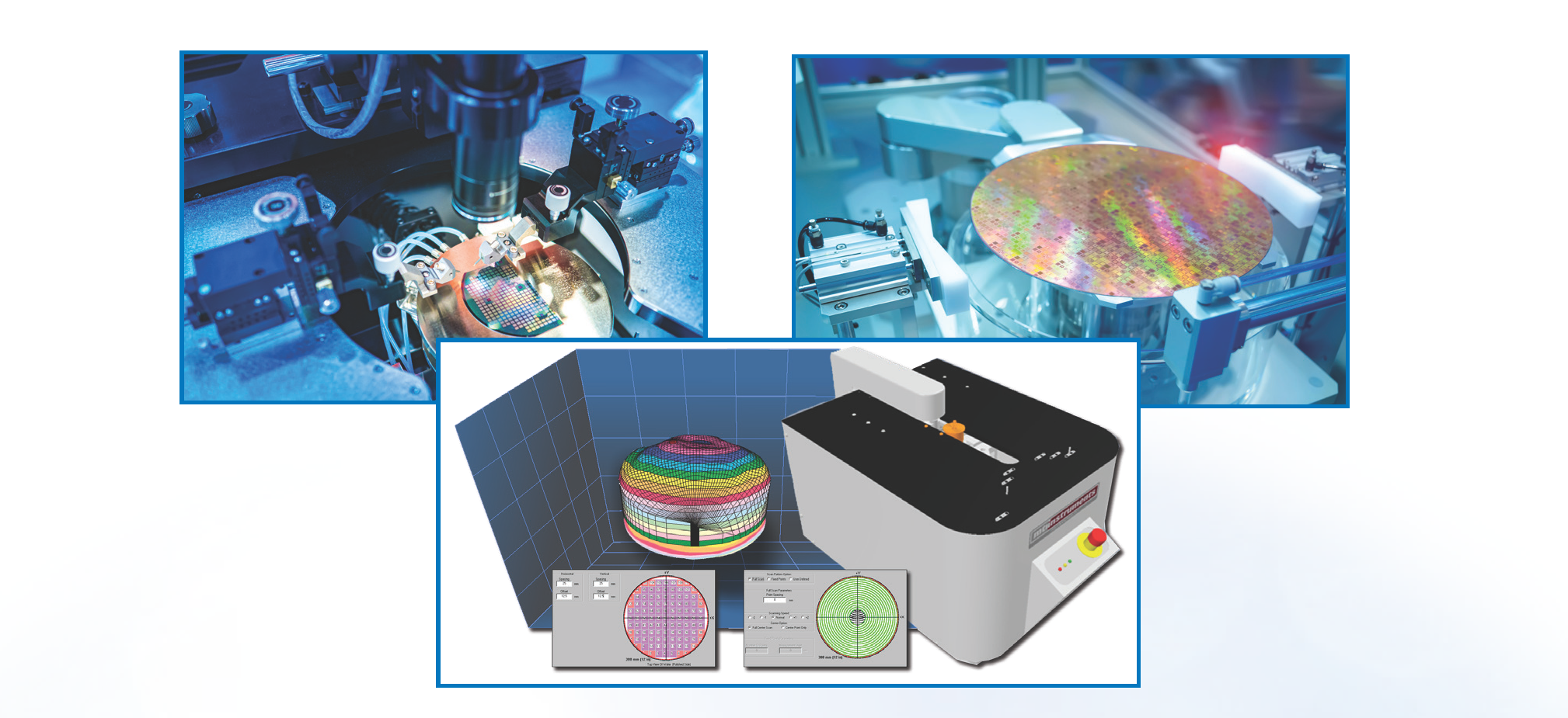
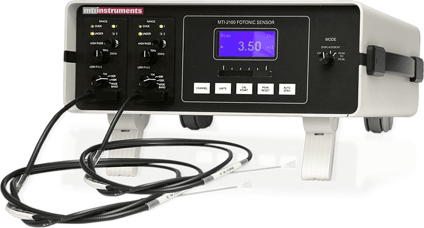
MTI Instruments of Lockport, IL makes manual and semi-automated non-contact wafer inspection and metrology systems that are capacitance-based. These systems can evaluate a thousand points per minute by measuring the ratio of change in an electric charge to the corresponding change in the electrical potential (i.e., voltage). MTI’s capacitance-based systems are also faster and more precise than more expensive optical systems that use a laser or beam of light.

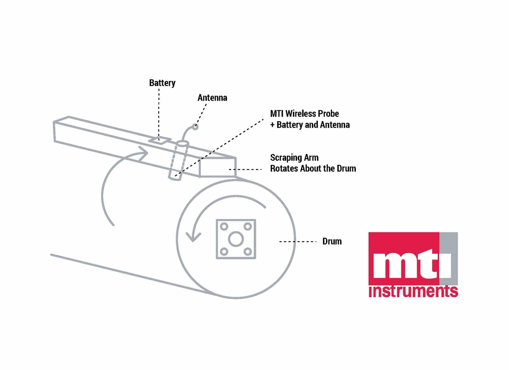
MTI’s Proforma technology uses two high-resolution non-contact capacitive probes to measure the distance from the probe to the wafer under test. One probe is on top and the other is under the wafer to measure the differential thickness. Because the probe’s sensing elements also provide some spatial averaging, this arrangement also works well with as-cut or unpolished wafers.

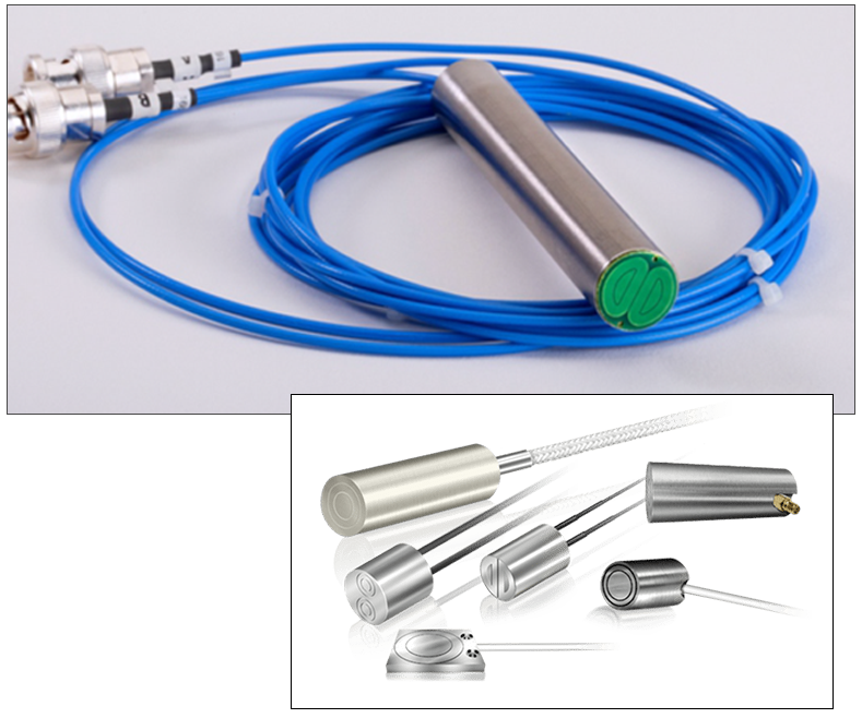
MTI’s proprietary push-pull™ probes do not require the wafer to be grounded. The probes also only measure to the surface of the wafer and are not affected by subsurface resistive or optical properties (i.e., transparency effects, such as with SiC). MTI’s Proforma systems can measure wafers up to 300 mm and in a wide range of disc sizes, thicknesses, and semiconductor material types.
The Proforma family of products includes two solutions for the semiconductor industry. Applications include qualifying new materials, quality control (QC), quality assurance (QA), and wafer sampling.
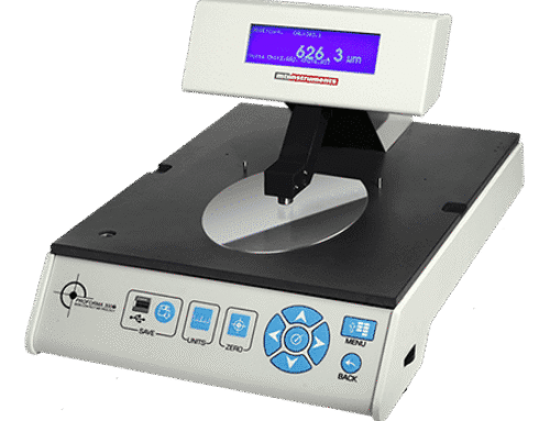
- The Proforma 300i is a manual metrology and inspection system that is a wafer thickness gauge and a differential measurement system that also measures bow.
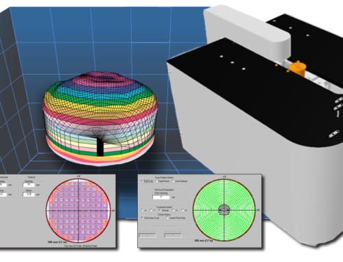
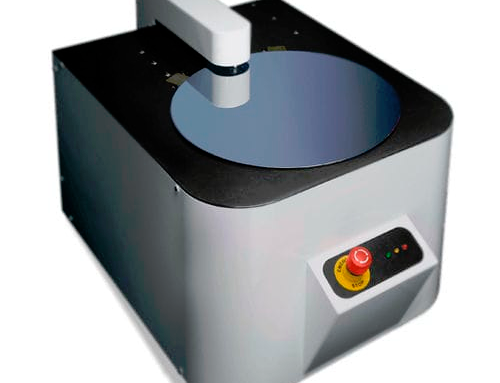
- The Proforma 300iSA is a semi-automatic system that provides full wafer surface scanning; delivers a more robust set of measurements, including both bow and warp; and supports stress analysis testing.
The Proforma 300i Manual Semiconductor Metrology System
 MTI’s Proforma 300i is a cost-effective choice for applications where a manufacturer needs a wafer thickness measurement. This manual system does not provide full-surface wafer scanning. Instead, it provides a point-based measurement from where the operator places a wafer between two fixed probes with a known fixed gap. The Proforma 300i measures wafers from 76 to 300 mm, has a measurement range up to 1700 µm, with an accuracy of ±0.25 µm. It can be used with the following types of semiconductor materials.
- silicon (Si)
- gallium arsenide (GaAs)
- germanium (Ge)
- indium phosphate (InP)
- silicon nitride (SiN)
- silicon carbide (SiC)
In addition to measuring substrate thickness, the Proforma 300i can measure five-point total thickness variation (TTV), the minimum and maximum thickness on the wafer. An optional feature, a bow wafer ring, allows for the measurement of bow, the deviation of the center point of the median surface of a free, un-clamped wafer from the reference plane.
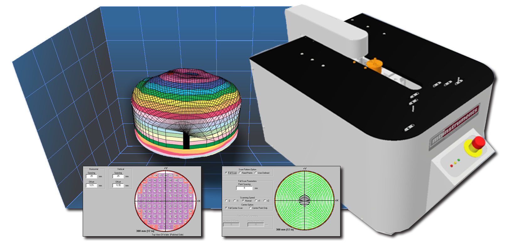
The Proforma 300iSA Semi-Automated Metrology System
 MTI’s Proforma 300iSA measures wafer thickness, TTV, and bow along with warp, site flatness, and global flatness. It also supports the use of parameters for comparative purposes and the indication of whether a wafer is out-of-specification. By looking at the entire median surface of the wafer instead of just the position at the center point, warp provides a more useful measurement of the true wafer shape. Flatness measurements are important to ensure that the wafer is suitable for lithographic processing. Otherwise, defective IC patterns can raise costs through waste.
The Proforma 300iSA has a measurement range of 100 to 1700 µm and an accuracy of ±0.25 µm. This semi-automated system can be used with the same materials as the Proforma 300i, including silicon carbide (SiC), an increasingly popular choice for applications such as the power electronics in electric vehicles (EVs). The Proforma 300iSA has up to a 1700 µm thickness range and can measure wafers with the following diameters.
- 76 mm
- 100 mm
- 125 mm
- 150 mm
- 200 mm
- 300 mm
Because MTI’s semi-automated system delivers full wafer surface scanning, it uses coordinates to indicate the region under inspection. Users can focus on a single quadrant or multiple quadrants, include or exclude the wafer’s edges or center, and also examine a defined number of points. The Proforma 300iSA can capture up to 1000 points per minute and can also output raw data for processing with other software for calculations and statistical analysis.
Finally, the Proforma 300iSA supports stress analysis for wafer characterization. During wafer processing, mechanical alterations can cause deformities that render the wafer unusable or out-of-specification. The Proforma 300iSA includes software for analyzing a wafer before and after processing to evaluate how its shape has changed. A thin film stress measurement calculation algorithm is also included. In the Analysis Area of the software, the user needs to know the semiconductor’s elasticity constant. Typically, this information is provided by the semiconductor supplier.
Metrology System Selection
MTI Instruments can help you to decide whether the Proforma 300i or the Proforma 300iSA is the right choice for your specific semiconductor wafer inspection and metrology application. As the Application Notes section of our website indicates, we have deep experience serving the semiconductor industry. For more information, contact us.


