
High Resolution Semiconductor Wafer Measurements at Lower Costs
MTI's Proforma technology characterizes semiconductor wafers in terms of bow and warp, thickness, total thickness variation (TTV) and center thickness. Until recently, semiconductor wafer measurements at resolutions less than 100 µm were cost-prohibitive. Moreover, only expensive devices such as interferometers were capable of these measurements. Today, the semiconductor industry can use capacitance gauges instead of laser interferometers to achieve high resolution at fraction of the cost. Much like affordable CCD cameras transformed and expanded the market for video, cost-effective capacitance is disrupting the semiconductor wafer measurement market and creating new opportunities for quality testing and validation. The [...]
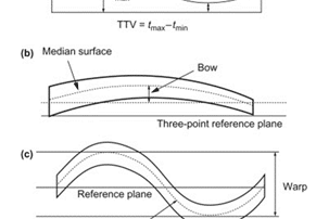 Measure Wafer Bow, Warp and TTV with Capacitance Gallery
Measure Wafer Bow, Warp and TTV with Capacitance
Application Notes-MTI, Brand-MTI, Industry-Battery, Industry-Compliance Testing, Industry-Consumer Products, Industry-Electronics, Industry-Manufacturing, Industry-Semiconductor, Industry-Semiconductor-MTI, Industry-Sensors, Products-MTI-Capacitance, Z-REPUB, z1, ZOK
Measure Wafer Bow, Warp and TTV with Capacitance
The flatness of silicon wafers used to manufacture integrated circuits is controlled to tight tolerances to help ensure that the whole wafer is sufficiently flat for lithographic processing. To ensure your wafer manufacturing process is within tolerance, you need to measure the wafers being produced. Various measurement techniques exist to verify process tolerances and eliminate expensive scrap wafers. Non-contact capacitive sensing is a highly precise and cost-effective means to measure wafer flatness, bow, warp, and total thickness variation (TTV). MTI Instruments’ Proforma 300i and 300iSA systems use capacitance sensors to improve yields while reducing costs through better dimensional control of [...]
Capacitance Sensing for Non-Contact Thickness Measurements of Insulating Materials
Capacitance sensing can be used to make non-contact thickness measurements for most insulating materials. Capacitance sensors are known for their ability to precisely measure the thickness and position of conductive targets, but what’s less known is that these sensors can also measure the thickness of non-conductive materials. Examples include glass, sapphire, and plastics, as well as semi-insulating semiconductor materials such as GaAs and silicon nitride. Analog vs. Digital Technologies MTI Instruments, a global supplier of precision measurement technologies, takes the guesswork out of what used to be a complex measurement for non-conductive materials. MTI's Digital Accumeasure system features a [...]
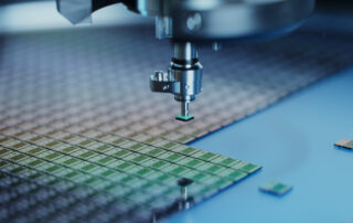 Trends in High Resolution Sensors for Semiconductor Metrology and Inspection Gallery
Trends in High Resolution Sensors for Semiconductor Metrology and Inspection
Application Notes-MTI, Brand-MTI, Industry-Compliance Testing, Industry-Consumer Products, Industry-Electronics, Industry-Manufacturing, Industry-Semiconductor, Industry-Semiconductor-MTI, Products-MTI-Capacitance, Products-MTI-Semiconductor/Metrology, Z-REPUB, z1
Trends in High Resolution Sensors for Semiconductor Metrology and Inspection
High resolution sensors are supporting improvements in semiconductor metrology and inspection at vital points in the production process. Because the fabrication of semiconductor wafers may require hundreds of steps and weeks of manufacturing time, early-stage defects that go undetected can have costly downstream consequences. Plus, because semiconductor processing always requires a high degree of precision, advances in fabrication methods seem to require ever-finer measurements in a never-ending quest. Today’s metrology instruments are incorporating high resolution sensors for automated wafer inspection. Resolution, the smallest measurement that a sensor can reliably indicate, may be given in dimensional units such as nanometers [...]

How to Reduce Inconsistent Wafer Measurements
How to Reduce Inconsistent Wafer Measurements Avoid 5 Common Mistakes That Destroy Wafer Measurement Accuracy You take pride in your work. You’re precise, accurate and depend on the right metrology equipment. Then why are your bare semi-conductor wafer measurements sometimes inconsistent? It may be something you’re doing (or not doing) — without realizing it. MTI Instruments discovered there are five common mistakes that engineers and users make with bare semi-conductor wafers. The “Five Mistakes Made When Taking Semiconductor Wafer Measurements” Tech-Brief details these all-too-typical errors that adversely impact measurements. [...]
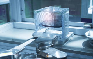 Five Common Mistakes with Semiconductor Wafer Measurement Gallery
Five Common Mistakes with Semiconductor Wafer Measurement
Application Notes-MTI, Brand-MTI, Industry-Compliance Testing, Industry-Consumer Products, Industry-Electronics, Industry-Manufacturing, Industry-Semiconductor, Industry-Semiconductor-MTI, Z-REPUB, z1
Five Common Mistakes with Semiconductor Wafer Measurement
Semiconductor wafer measurement requires a high degree of precision. The right metrology equipment and inspection processes are important, but so is procedural consistency and attention to detail. If you’re not getting the results you want, it’s time to look beyond the measurements. With bare semiconductor wafers, users need to avoid these five common mistakes. Mistake #1 | Turning the Device Off Most users turn on metrology devices only when it’s time to use them. As soon as semiconductor wafer measurement is complete, the devices are turned off. This reduces electricity consumption but also introduces thermal instability that can cause [...]
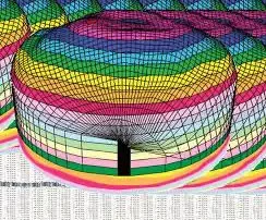 Proforma 300i SA Video Shows Semiconductor Metrology Gallery
Proforma 300i SA Video Shows Semiconductor Metrology
Brand-MTI, Industry-Compliance Testing, Industry-Consumer Products, Industry-Electronics, Industry-Manufacturing, Industry-R&D, Industry-Semiconductor, Industry-Semiconductor-MTI, New & Press Releases, News-MTI-Metrology, News-Product Updates, Press Releases-Vitrek, Products-MTI-Semiconductor/Metrology, Videos-MTI, Videos-MTI-Manual Semiconductor Metrology System, Z-REPUB, z1
Proforma 300i SA Video Shows Semiconductor Metrology
MTI Instruments, a worldwide leader in precision measurement solutions, has released a YouTube video that shows how its Proforma™ 300i SA semi-automated measurement tool measures silicon carbide wafers for semiconductors. George Relan, MTI’s Global Director of Sales, demonstrates how the desktop metrology system provides non-contact full wafer scanning and 3D mapping of measurement features such as thickness and shape. MTI’s video also shows how the Proforma 300i SA interfaces with an external computer and provides powerful Windows-based software for analysis and reporting. By utilizing MTI push/pull technology, the Proforma 300i SA doesn’t require the semiconductor wafers to have a [...]
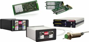 3D Integrated Circuits Use Capacitive Sensing to Ensure Coplanarity Gallery
3D Integrated Circuits Use Capacitive Sensing to Ensure Coplanarity
Application Notes-MTI, Brand-MTI, Industry-Consumer Products, Industry-Electronics, Industry-Manufacturing, Industry-Semiconductor, Industry-Semiconductor-MTI, Industry-Sensors, Z-REPUB, z1
3D Integrated Circuits Use Capacitive Sensing to Ensure Coplanarity
Three-dimensional (3D) integrated circuits (ICs) feature silicon wafers and dies that are stacked vertically for improved device performance. By using the Z-axis, 3D ICs can overcome the power and footprint limitations associated with two-dimensional (2D) integrated circuits. Yet 3D ICs need coplanar surfaces to contact all of the pads, pins, and pillars. To determine coplanarity, semiconductor manufacturers measure the angle and gap between two planes. Bonding tool actuators use these measurements to adjust components and ensure that all device pins and solder balls reside on the same geometric plane. This process, active parallelism compensation, promotes proper bonding without residual [...]



About Wafer Bow And Warp Measurement Systems
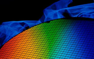
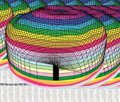
About Wafer Bow And Warp Measurement Systems Semiconductor/Solar Wafer Bow And Warp Metrology/Surface Thickness Measurement for Metrology Systems ASTM F657: The distance through a wafer between corresponding points on the front and back surface. Thickness is expressed in microns or mils (thousandths of an inch). Total Thickness Variation (TTV) ASTM F657: The difference between the maximum and minimum values of thickness encountered during a scan pattern or series of point measurements. TTV is expressed in microns or mils (thousandths of an inch). Figure above shows a wafer placed between two non-contact [...]