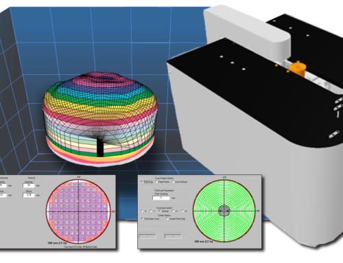
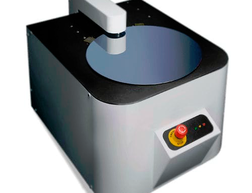
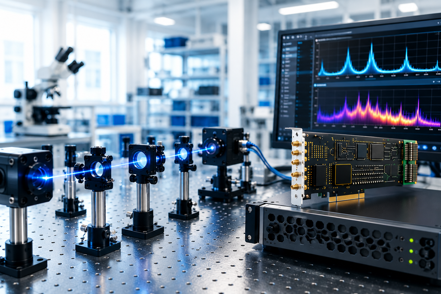
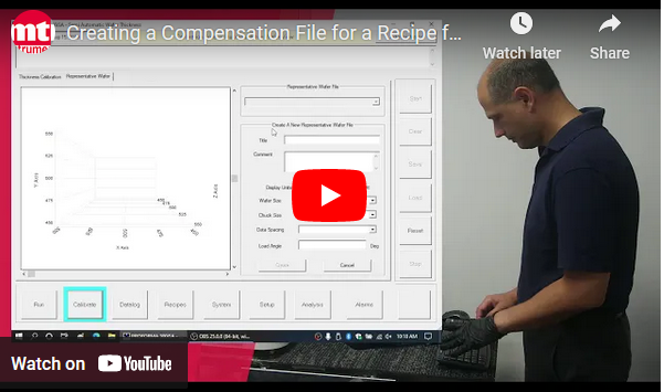
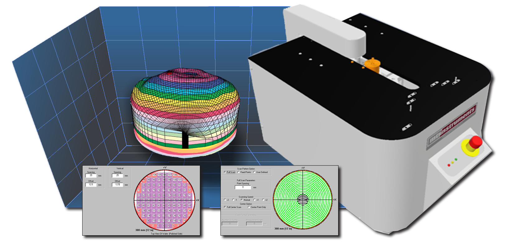
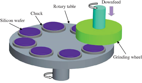
 MTI Instruments, a worldwide leader in precision measurement solutions, has released a YouTube video that shows how its Proforma™ 300i SA semi-automated measurement tool measures silicon carbide wafers for semiconductors. George Relan, MTI’s Global Director of Sales, demonstrates how the desktop metrology system provides non-contact full wafer scanning and 3D mapping of measurement features such as thickness and shape.
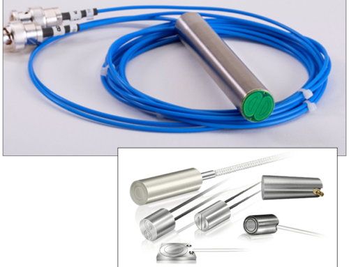
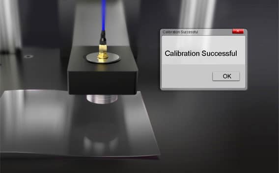
MTI’s video also shows how the Proforma 300i SA interfaces with an external computer and provides powerful Windows-based software for analysis and reporting. By utilizing MTI push/pull technology, the Proforma 300i SA doesn’t require the semiconductor wafers to have a consistent electrical ground. This desktop metrology system includes full remote-control operation and Ethernet network interface capability.
Measuring Silicon Carbide Wafers with Proforma 300i Technology
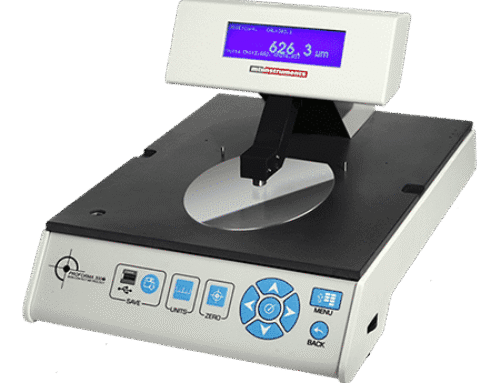
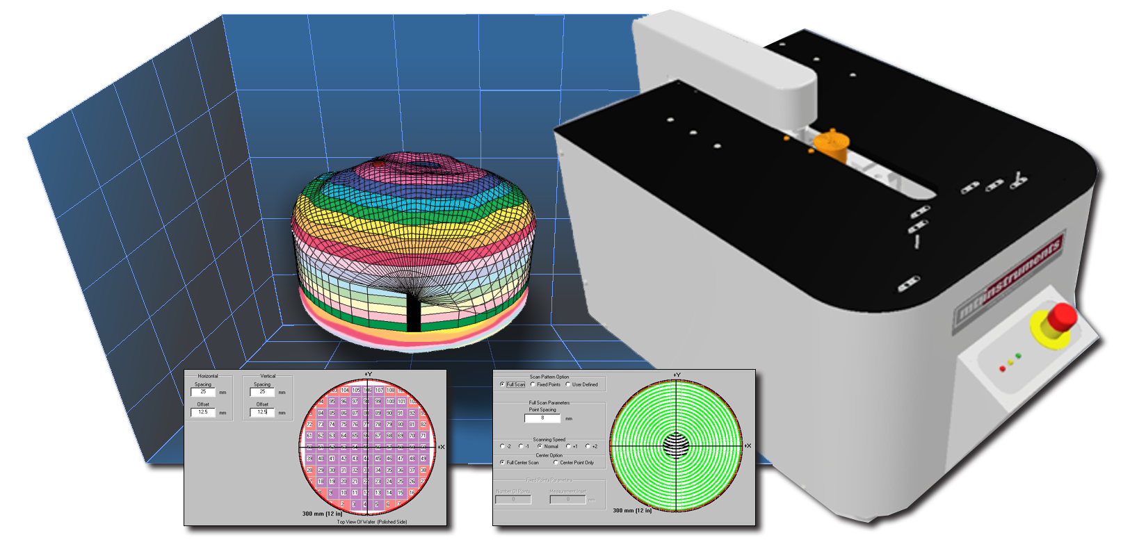
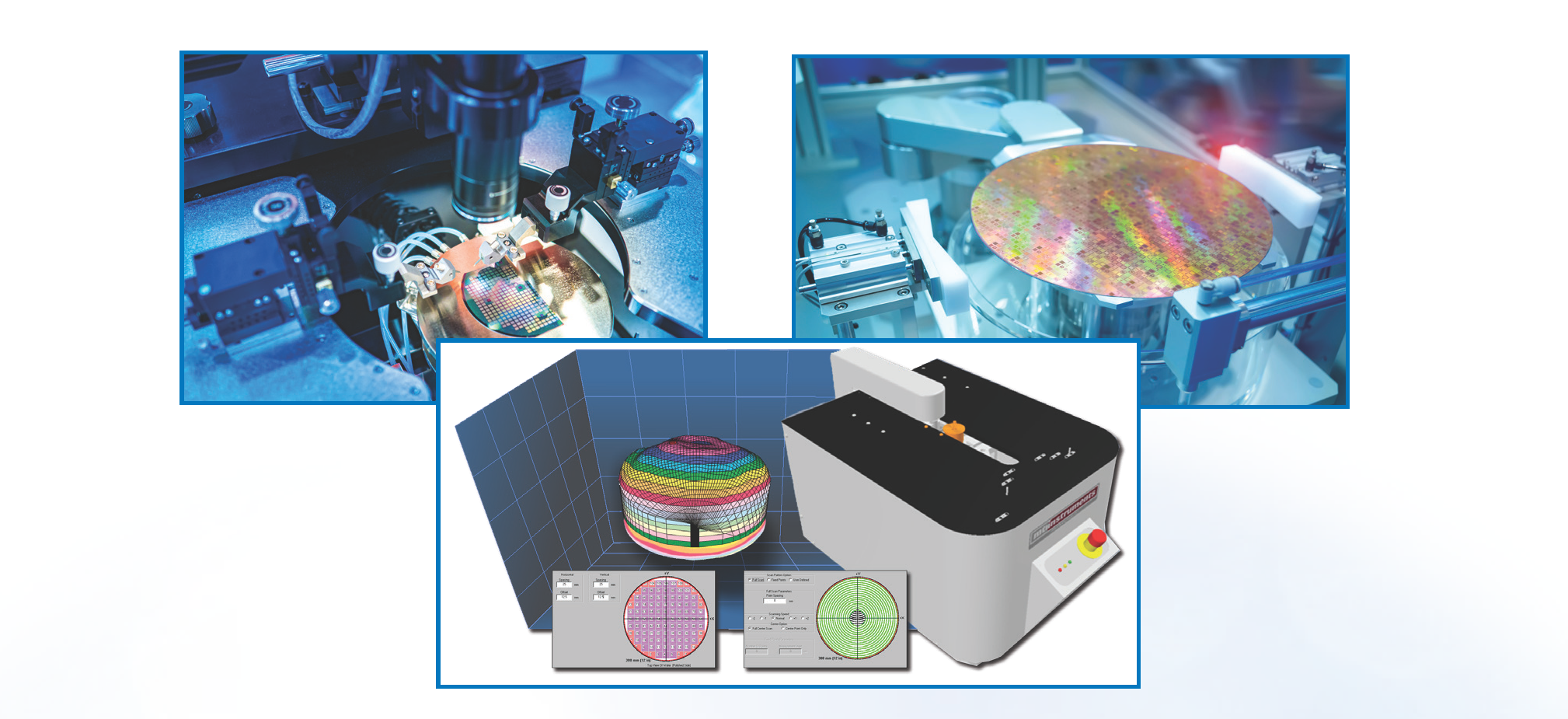
Silicon carbide or SiC wafers are used in electronics applications and in the automotive industry. These semiconductor wafers need to meet highly-precise requirements for thickness, shape, and flatness. Bow and warp are important measures of flatness. The Proforma 300SA delivers full wafer surface scanning for thickness, thickness variation, bow, warp, site and global flatness. As MTI’s video shows, it’s a misconception that capacitance-based technologies can’t measure these semiconductor wafers.
Because the Proforma 300i SA is semi-automated, an operator simply loads the semiconductor wafer onto the measurement stage and then presses a button on the machine. After 30 seconds of measurement, the Proforma 300i SA stops. The measurements are displayed on an external computer that’s interfaced to the desktop metrology system. Windows-based software shows detailed information about the wafer. User-defined and ASTM/SEMI compliant scan patterns are used to generate full 3D wafer images.
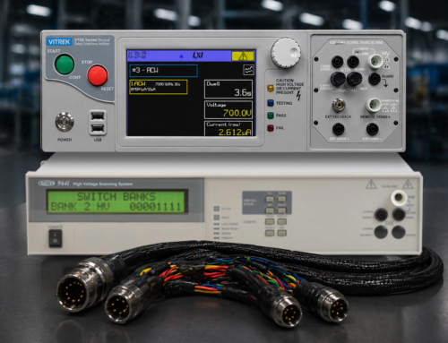
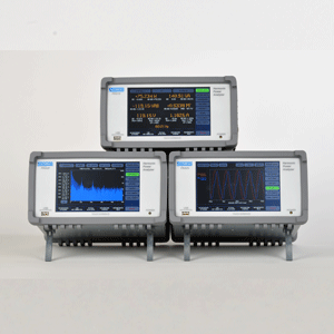
Proforma 300i Desktop Metrology System
The Proforma 300i SA semi-automated wafer inspection and metrology system can measure as-cut, lapped, etched, polished or pattern wafers against a semiconductor manufacturer’s “recipe”. The system comes preset for SEMI standard wafer diameters and offers the ability to add custom wafer parameters. To support “what-if” engineering analysis, parameters can be modified and data recalculated without the need to rescan the wafer.”
For more information about the Proforma 300i SA, download the brochure.


