Wafer Stress Analysis Using the 300iSA
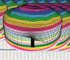
Wafer Stress Analysis Using MTI Instruments Proforma 300iSA Wafer processing involves several stages that can lead to mechanical changes in the wafer structure. These changes, or stresses, may result in deformities, making the wafer either unusable or only marginally usable. To evaluate these stresses and determine the wafer's quality, wafer stress measurement is essential. The Proforma 300iSA wafer characterization tool offers a powerful solution for wafer stress analysis. It allows for the analysis of a wafer both before and after processing. By comparing these two states, the Proforma 300iSA effectively evaluates the wafer's stress levels and mechanical alterations, providing [...]
 Wafer Backgrinding and Semiconductor Thickness Measurements Gallery
Wafer Backgrinding and Semiconductor Thickness Measurements
Application Notes-MTI, Brand-MTI, Industry-Compliance Testing, Industry-Consumer Products, Industry-Electronics, Industry-Manufacturing, Industry-Semiconductor, Industry-Semiconductor-MTI, News-MTI-Instrumentation, News-MTI-Metrology, Products-MTI-Capacitance, Products-MTI-Semiconductor/Metrology, Z-REPUB, z1

Wafer Backgrinding and Semiconductor Thickness Measurements
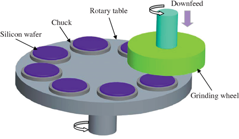
Wafer Backgrinding and Thickness Measurements in Semiconductor Manufacturing Wafer backgrinding, also known as wafer thinning or wafer lapping, is a critical step in semiconductor packaging. This process, which involves grinding the backside of a semiconductor wafer, reduces its thickness to enable the stacking of integrated circuits (ICs) and support high-density packaging. The thickness of the wafer plays a crucial role in determining the overall size of the package, an important factor as modern electronics such as smartphones, laptops, and other devices continue to get thinner and more compact. In applications like MEMS (Micro-Electro-Mechanical Systems), the backgrinding process also affects [...]
 Transducer Selection for High Resolution Applications Gallery
Transducer Selection for High Resolution Applications
Application Notes-MTI, Brand-MTI, News-MTI-Instrumentation, News-MTI-Metrology, News-Product Updates, News-Products, Products-MTI-Capacitance, Products-MTI-Laser/Fiber Optic, Products-MTI-Semiconductor/Metrology, Products-MTI-Signal Generators, Z-REPUB, z1
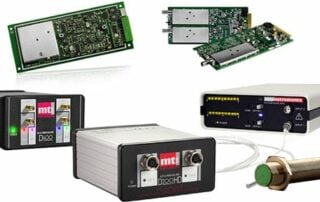
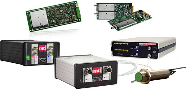
Transducer Selection for High Resolution Applications
High resolution applications do not always require an interferometer. If you want to make accurate measurements in the micron to picometer range, then an MTI Digital Accumeasure D100 HD or D200 system may be what you need. Laser interferometers can sell for more than $15,000 and be difficult to setup. For example, you may have to buy additional optics to guarantee a good return signal since the laser beam must reflect off a mirror surface or precision retro reflector in order for the beam to re-enter the interferometer’s optics at less than a degree of reflection angle. The downsides [...]
Capacitance Sensing for Non-Contact Thickness Measurements of Insulating Materials
Capacitance sensing can be used to make non-contact thickness measurements for most insulating materials. Capacitance sensors are known for their ability to precisely measure the thickness and position of conductive targets, but what’s less known is that these sensors can also measure the thickness of non-conductive materials. Examples include glass, sapphire, and plastics, as well as semi-insulating semiconductor materials such as GaAs and silicon nitride. Analog vs. Digital Technologies MTI Instruments, a global supplier of precision measurement technologies, takes the guesswork out of what used to be a complex measurement for non-conductive materials. MTI's Digital Accumeasure system features a [...]
 Capacitance Sensing Provides Two Ways to Measure EV Battery Plate Thickness Gallery
Capacitance Sensing Provides Two Ways to Measure EV Battery Plate Thickness
Application Notes-MTI, Brand-MTI, Industry-Automotive, Industry-Energy, Industry-Manufacturing, News-MTI, News-MTI-Instrumentation, News-MTI-Metrology, News-Product Updates, Products-MTI-Capacitance, Products-MTI-Laser/Fiber Optic, Products-MTI-Semiconductor/Metrology, Z-REPUB, z1
Capacitance Sensing Provides Two Ways to Measure EV Battery Plate Thickness
MTI Instruments has released an application note that explains how to use capacitance to measure the thickness of the lithium battery plates in electric vehicles (EVs). Manufacturers need to check these plates for thickness before calendaring them together to ensure that the overall battery diameter is within specifications. In EV batteries, lithium ion compounds are applied to either a copper plate substrate (cathode) or an aluminum substrate (anode plate). These conductive plates are separated by a dielectric. MTI Instruments, a global supplier of precision measurement solutions, makes capacitance sensors that can measure thicknesses materials down to nanometers. Moreover, MTI [...]
 Proforma 300i SA Video Shows Semiconductor Metrology Gallery
Proforma 300i SA Video Shows Semiconductor Metrology
Brand-MTI, Industry-Compliance Testing, Industry-Consumer Products, Industry-Electronics, Industry-Manufacturing, Industry-R&D, Industry-Semiconductor, Industry-Semiconductor-MTI, New & Press Releases, News-MTI-Metrology, News-Product Updates, Press Releases-Vitrek, Products-MTI-Semiconductor/Metrology, Videos-MTI, Videos-MTI-Manual Semiconductor Metrology System, Z-REPUB, z1
Proforma 300i SA Video Shows Semiconductor Metrology
MTI Instruments, a worldwide leader in precision measurement solutions, has released a YouTube video that shows how its Proforma™ 300i SA semi-automated measurement tool measures silicon carbide wafers for semiconductors. George Relan, MTI’s Global Director of Sales, demonstrates how the desktop metrology system provides non-contact full wafer scanning and 3D mapping of measurement features such as thickness and shape. MTI’s video also shows how the Proforma 300i SA interfaces with an external computer and provides powerful Windows-based software for analysis and reporting. By utilizing MTI push/pull technology, the Proforma 300i SA doesn’t require the semiconductor wafers to have a [...]