Wafer Backgrinding and Thickness Measurements in Semiconductor Manufacturing
Wafer backgrinding, also known as wafer thinning or wafer lapping, is a critical step in semiconductor packaging. This process, which involves grinding the backside of a semiconductor wafer, reduces its thickness to enable the stacking of integrated circuits (ICs) and support high-density packaging. The thickness of the wafer plays a crucial role in determining the overall size of the package, an important factor as modern electronics such as smartphones, laptops, and other devices continue to get thinner and more compact.
In applications like MEMS (Micro-Electro-Mechanical Systems), the backgrinding process also affects critical parameters such as the proof mass for accelerometers and diaphragm thickness for pressure sensors. The goal of wafer backgrinding is to reduce the wafer’s thickness while preserving the integrity of the wafer structure for precise assembly.
Understanding the Wafer Backgrinding Process
The wafer backgrinding process involves placing a wafer on a rotary table, with its backside facing down toward a rotating lapping surface. This surface gradually removes the excess material to achieve the desired thickness. For instance, a typical semiconductor wafer starts at a thickness of about 775 µm. However, the ground thickness varies depending on the device application:
- Logic gates often require wafers with a thickness of around 100 µm.
- DRAM memory wafers are generally thinned to around 50 µm.
- MEMS wafers typically have a thickness of approximately 30 µm.
Precision is key during the wafer backgrinding process, but the grinding can damage the wafer’s surface. To address this, the wafer undergoes polishing to remove any residual damage. While this explanation offers an overview of the wafer backgrinding process, it’s essential to note that each step of semiconductor fabrication, including wafer thinning, is tightly controlled to meet exact specifications.

Source: Semantic Scholar
Wafer Thickness and Measurement Accuracy
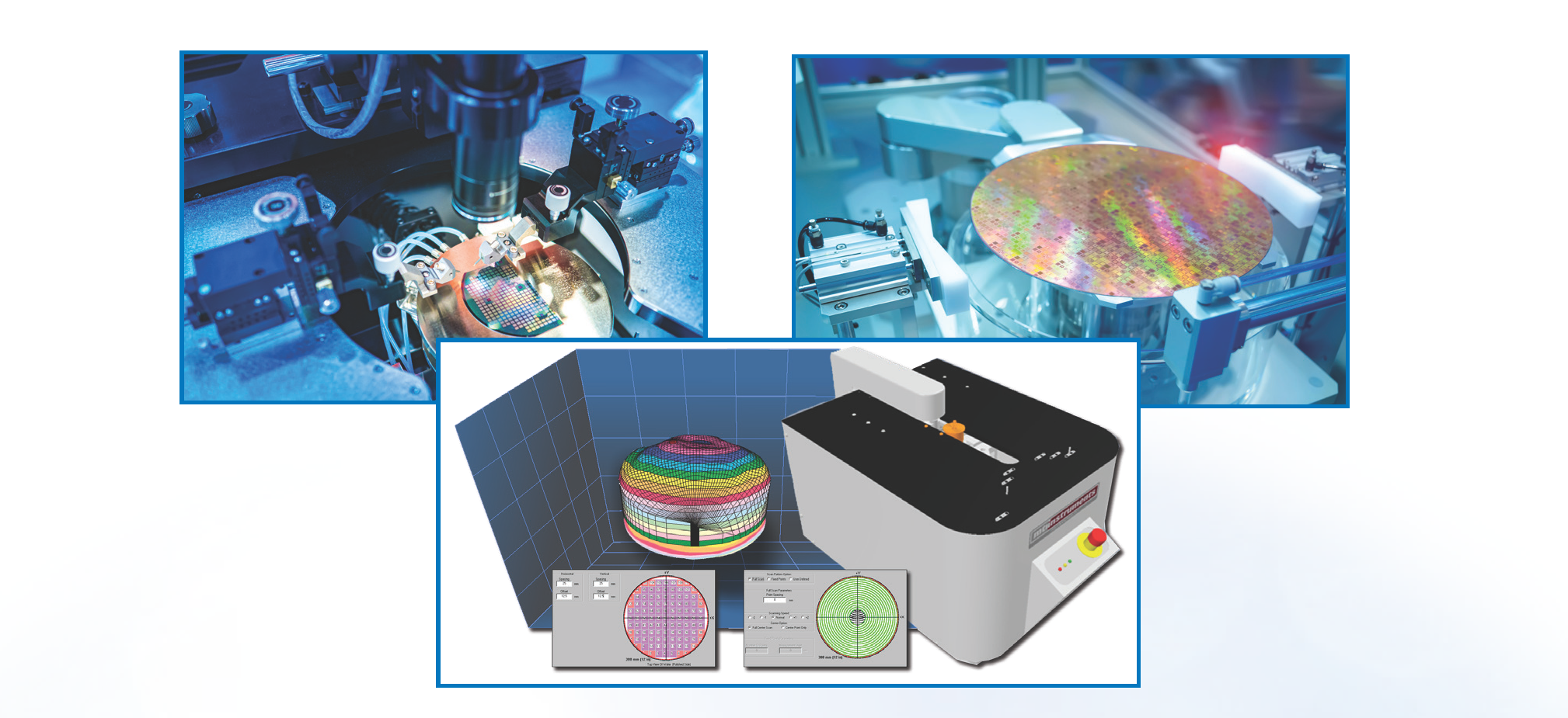
Wafer thickness measurements, including Total Thickness Variation (TTV), bow, warp, sori, and flatness, are essential during the semiconductor manufacturing process. Accurate measurements of wafer thickness are crucial before processes like lithography, as any deviation could lead to inefficiencies or manufacturing waste. This is especially important considering that a finished 300 mm semiconductor wafer can be valued at thousands of dollars.
Companies that produce wafer backgrinding equipment also rely on high-precision thickness measurements to ensure the material is correctly removed to achieve the target wafer thickness. Manufacturers of wafers often take precise measurements before shipping, and customers may recheck the thickness upon receipt to ensure compliance.

Source: MTI Instruments
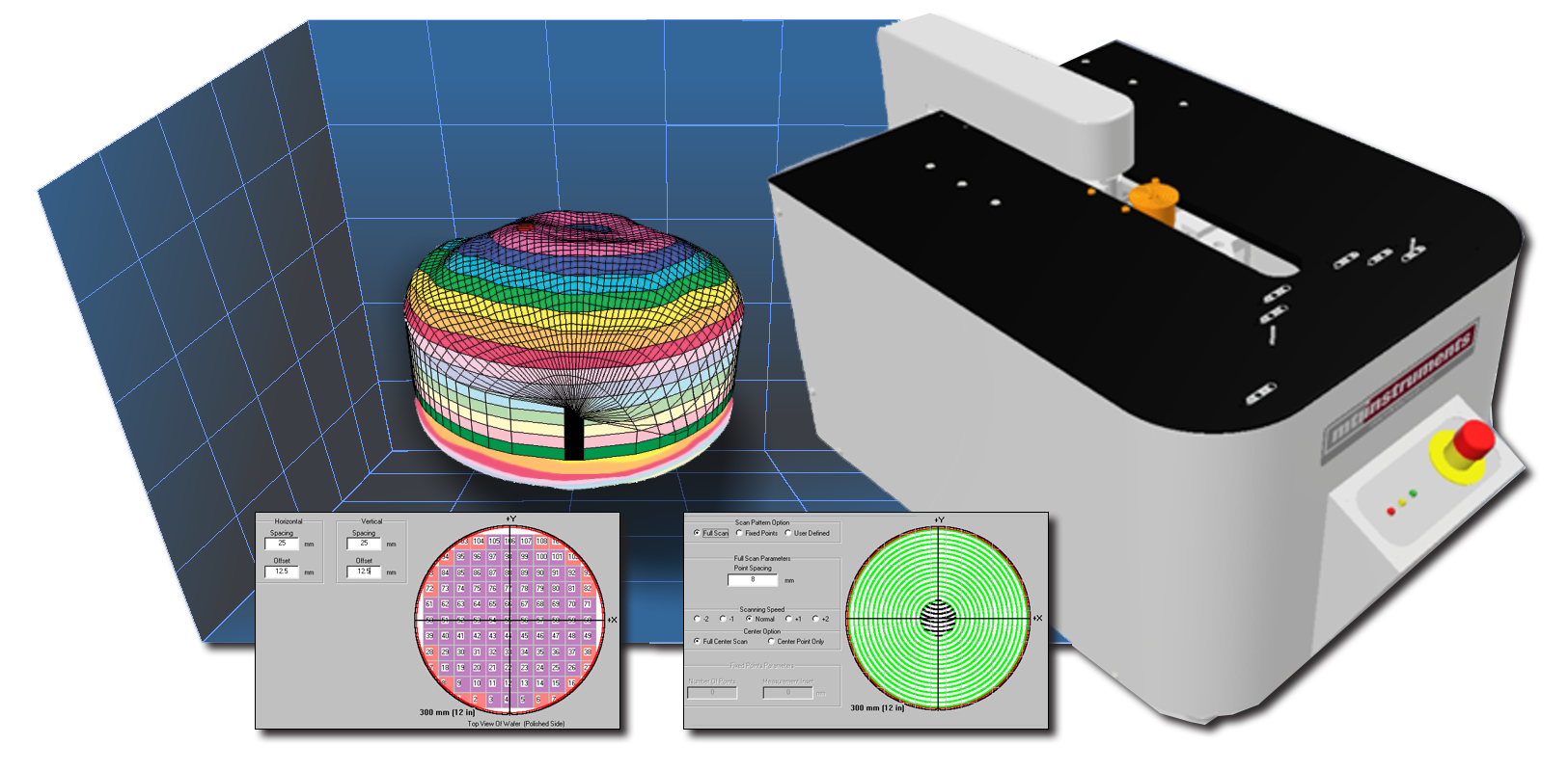
Wafer Thickness Measurement Tools: Laser Interferometers vs. Capacitance Gauges
In the semiconductor industry, thickness measurement tools such as laser interferometers and capacitance gauges are vital for ensuring wafer precision. While laser interferometers provide high-resolution measurements, they rely on relative readings, meaning the operator must calibrate them to a known thickness beforehand. However, capacitance gauges offer absolute measurements for greater accuracy, making them a more cost-effective solution. These gauges are available as off-line devices and are often used in semiconductor manufacturing.
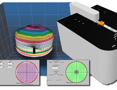
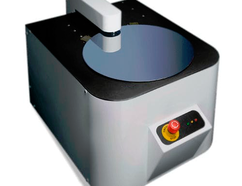
Capacitance Gauging Systems for Accurate Wafer Measurements
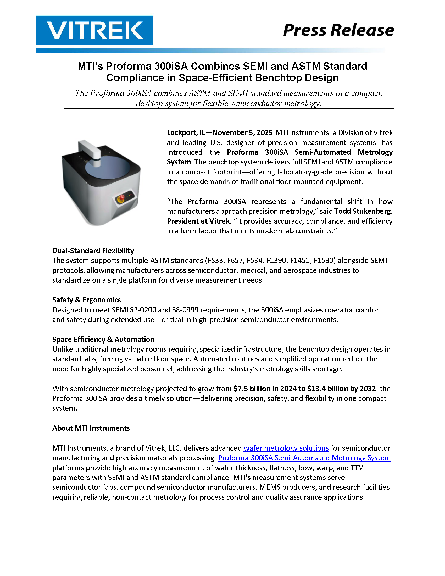
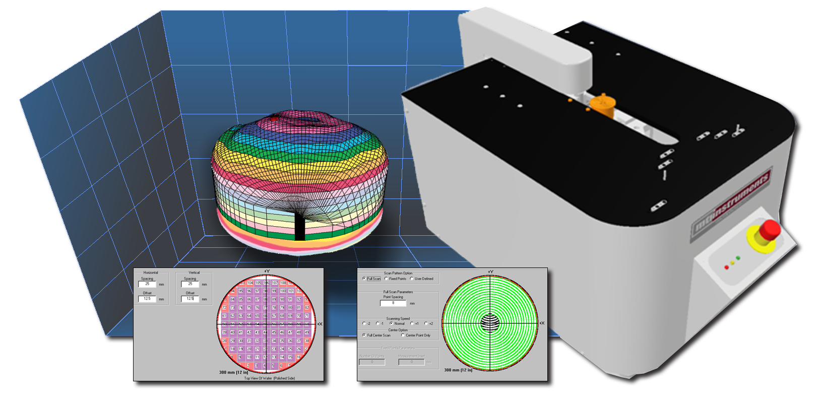
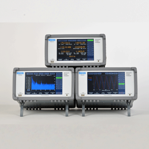
MTI Instruments offers capacitance-based systems like the Proforma 300i and 300iSA, which are used for quality control in wafer backgrinding processes. These systems are less expensive than laser interferometers and provide absolute measurements. Available in manual (300i) and semi-automated (300iSA) configurations, these systems support early-stage quality checks in the semiconductor supply chain. By integrating them into the wafer manufacturing process, companies can achieve higher efficiency and cost savings.

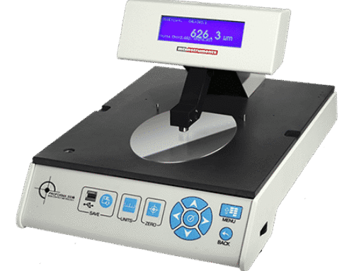
MTI Semi-Automated Proforma 300iSA Thickness Metrology Tool (Left)
MTI Proforma 300 Manual Thickness Tool (Right)
Source: MTI Instruments
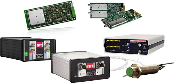
Advanced Measurement Solutions: Digital Accumeasure for Sub-Micron Accuracy
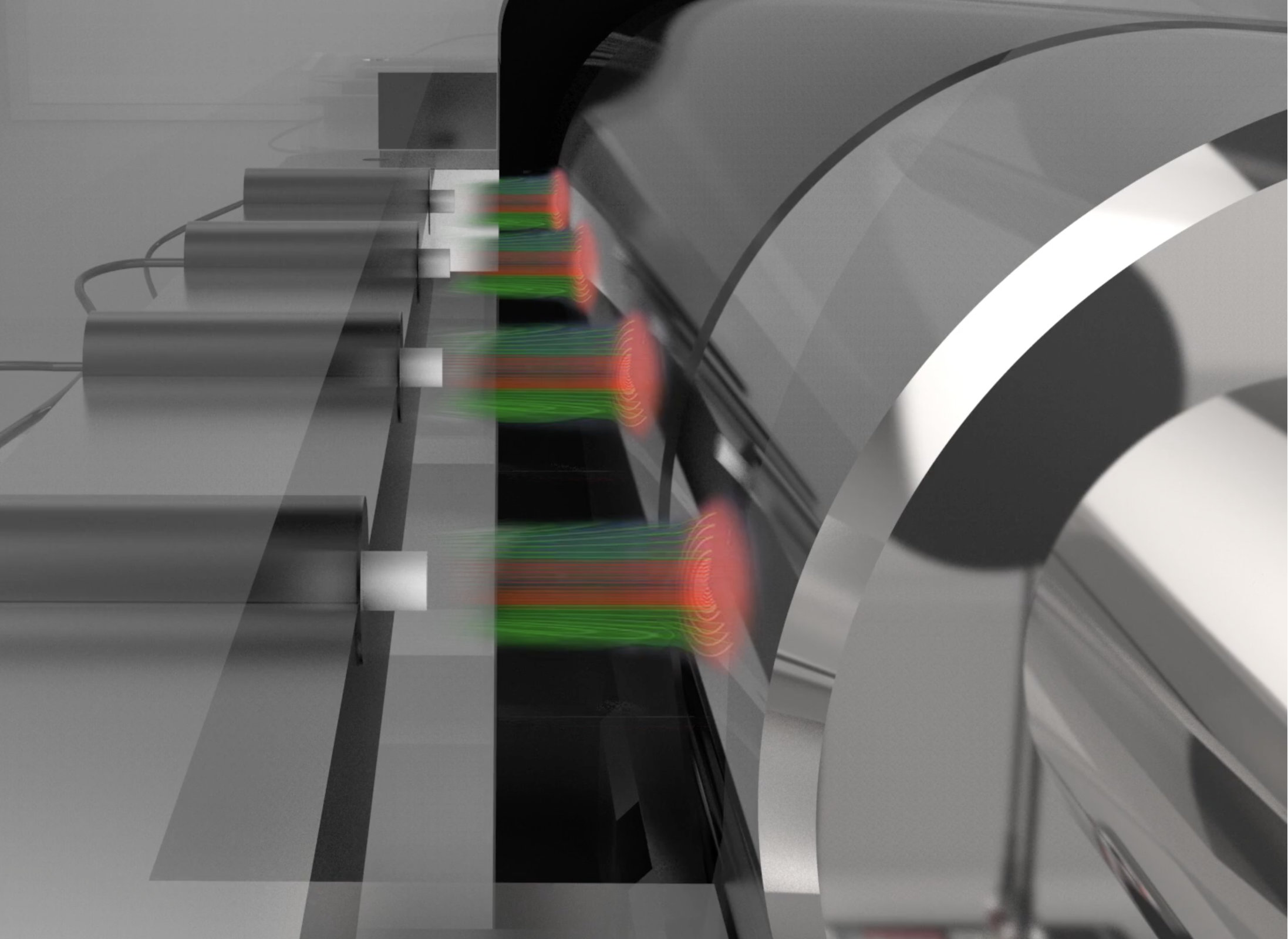
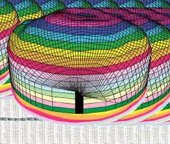
For highly accurate measurements below one micron, MTI’s Digital Accumeasure system offers a capacitance-based, non-contact measurement solution. This stand-alone amplifier with probes can be integrated into various measurement processes or OEM systems. The system is capable of measuring not only wafer thickness but also TTV, bow, and warp. Calibration is user-friendly, and the digital filtering function provides further flexibility. The measured data is compatible with standard PC software, making integration into existing processes seamless.

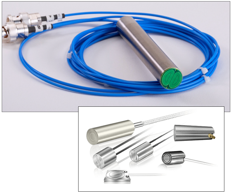
Four-channel MTI Accumeasure D with two Push-Pull probes can measure wafer thickness non-contact
Source: MTI Instruments

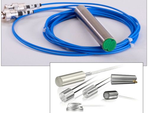
MTI Push-Pull Non-Contact Probe
Source: MTI Instruments
For more information about our advanced solutions for semiconductor wafer measurement and precision thickness control, contact MTI Instruments today.


