 Contact vs. Non-Contact Measurement and Linear Displacement Sensors Gallery
Contact vs. Non-Contact Measurement and Linear Displacement Sensors
Application Notes-MTI, Brand-MTI, Industry-Compliance Testing, Industry-Consumer Products, Industry-Electronics, Industry-Manufacturing, Industry-Semiconductor, Industry-Semiconductor-MTI, Industry-Sensors, Products-MTI-Capacitance, Z-REPUB, z1, ZOK
Contact vs. Non-Contact Measurement and Linear Displacement Sensors
Contact vs. Non-Contact Measurements Choosing between a contact measurement system and a non-contact measurement system requires careful evaluation of your application’s performance needs, material properties, environmental conditions, and measurement goals. Each system type offers unique advantages- and understanding these distinctions can help you make a more informed decision. Let's explores how contact and non-contact measurement techniques work, their strengths and limitations, and where they’re best applied. What Are Contact Measurement Systems? Contact measurement systems involve tools and sensors that physically touch the object to determine various physical characteristics. These systems are widely used in dimensional metrology, offering high precision, [...]
Capacitance Sensors vs. Eddy Current Sensors Application Note
Capacitance Sensors vs. Eddy Current Sensors Application Note Capacitance sensors and Eddy current sensors are both used for non-contact measurements. Capacitive probes use electric fields to measure the distance from the sensor face to the surface of a target that is typically conductive and grounded. Eddy current probes use an alternating AC current to induce a magnetic field in a conductive target instead. In turn, the induced magnetic field produces a back magnetic field that is proportional to the gap between the probe face and the target. In a recent application note, MTI Instruments examines the differences between capacitance [...]
Foam Density Measurement: Capacitance Sensors vs. Nuclear Gauges
This application note from MTI Instruments compares two technologies for measuring foam density: capacitance sensors and nuclear gauges. It examines the basic operating principles of each technology and explains why capacitance measurement is recommended for in-line measurement during foam manufacturing. Capacitance Sensors Capacitive probes are non-contact devices that use electric fields to measure foam density. In combination with a thickness value, a density measurement may be calculated. These probes consist of a capacitance sensor inside of a protective housing and are part of a larger measurement system that includes amplifiers, cables, and software. With parallel plate capacitance, the capacitance probe [...]
Capacitance Sensing vs. Strain Gauge Sensing Application Note
Capacitance Sensing vs. Strain Gauge Sensing Application Note Capacitance probes that are embedded in piezo flexure stages can provide significantly greater accuracy than strain gauges. Although some minor mounting modifications are required, capacitance probes with picoscale positioning provide higher linearity, greater long-term stability, and better direct measurement. Capacitance sensors cost more, however, and are limited by sensing distance. Therefore, strain gauge sensors remain a good choice for applications where cost is a consideration, sensing distances are larger, and high resolution or high accuracy are required. In a recent application note, MTI Instruments examines the differences between capacitance probes and [...]
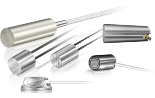
 Using Capacitance Sensors for Non-Conductive Material Measurement Gallery
Using Capacitance Sensors for Non-Conductive Material Measurement
Application Notes-MTI, Brand-MTI, Industry-Compliance Testing, Industry-Consumer Products, Industry-Electronics, Industry-Manufacturing, Industry-Sensors, News-MTI, News-MTI-Instrumentation, Products-MTI-Capacitance, Z-REPUB, z1
Using Capacitance Sensors for Non-Conductive Material Measurement
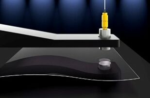
Non-Conductive Material Measurement with Capacitance Sensors Capacitance sensors are non-contact devices that can be used to obtain position, thickness, and dynamic measurements with a high degree of precision, accuracy, and resolution. Capacitive measurement is used with electrically-conductive materials such as metals but can also be used to measure non-conductive materials such as glass, sapphire, and many plastics. Even if a non-conductive material is relatively inexpensive (such as closed cell foam), manufacturers want to avoid errors that can result in significant waste across high volumes. Importantly, capacitance measurement is also used with semi-insulating materials such as gallium arsenide (GaAs) and [...]
 Why Demand for SiC Wafers is Soaring and Durable Gallery
Why Demand for SiC Wafers is Soaring and Durable
Brand-MTI, Industry-Consumer Products, Industry-Electronics, Industry-Manufacturing, Industry-Semiconductor, Industry-Semiconductor-MTI, MTI Blog, News-MTI, News-MTI-Metrology, Products-MTI-Semiconductor/Metrology, Z-REPUB, z1
Why Demand for SiC Wafers is Soaring and Durable
Silicon carbide (SiC) wafers are in high demand, particularly in high-temperature applications. Silicon carbide (SiC), a semiconductor material made of both silicon and carbon, can withstand extreme temperatures of up to 2700°C. Often referred to as carborundum, SiC’s unique properties also make it a key material in non-electronic applications such as bulletproof vests, extrusion dies, sandpaper, and high-performance disc brakes. In the electronics industry, SiC wafers are crucial for devices operating under high temperatures, high voltages, or both. For example, they are used in electric vehicle (EV) power electronics, 5G communication systems, and LED technology, making SiC a material [...]
Wafer Stress Analysis Using the 300iSA
Wafer Stress Analysis Using MTI Instruments Proforma 300iSA Wafer processing involves several stages that can lead to mechanical changes in the wafer structure. These changes, or stresses, may result in deformities, making the wafer either unusable or only marginally usable. To evaluate these stresses and determine the wafer's quality, wafer stress measurement is essential. The Proforma 300iSA wafer characterization tool offers a powerful solution for wafer stress analysis. It allows for the analysis of a wafer both before and after processing. By comparing these two states, the Proforma 300iSA effectively evaluates the wafer's stress levels and mechanical alterations, providing [...]

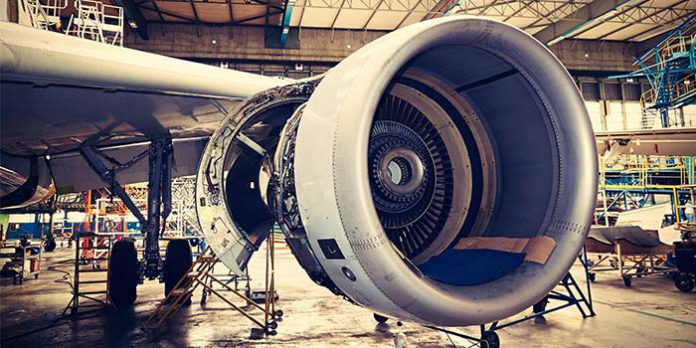
Weathering the storm: Keys to resiliency in MRO
Weathering the storm: Keys to resiliency in MRO By Ken Ameika It’s no secret that COVID-19 has adversely affected the airline industry, and consequently the MRO and test cell markets. But the impacts are nuanced. Commercial aircraft utilization is way down; meanwhile, freight carrier business is expanding markedly. Operators are spending less; but they still have needs, which often require quick turnaround. It’s been hard for many. But there’s good news: COVID provided lessons that we can all use to make our businesses, or our careers, more resilient to the next major disruption. Diversify Your Business Commercial passenger traffic—or [...]
 CMP and Capacitance-Based Semiconductor Wafer Measurement Gallery
CMP and Capacitance-Based Semiconductor Wafer Measurement
Application Notes-MTI, Brand-MTI, Industry-Compliance Testing, Industry-Consumer Products, Industry-Electronics, Industry-Manufacturing, Industry-Semiconductor, Industry-Semiconductor-MTI, Industry-Sensors, Products-MTI-Capacitance, Products-MTI-Semiconductor/Metrology, z1
CMP and Capacitance-Based Semiconductor Wafer Measurement
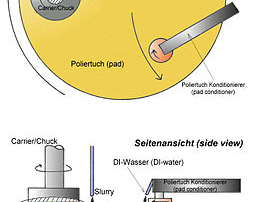
Chemical mechanical polishing (CMP) uses chemical oxidation and mechanical abrasion to selectively remove material from semiconductor wafers in order to achieve very high levels of planarity. The planarity, or flatness, of these wafers is important for optical lithography, a microfabrication technique that produces integrated circuits (ICs) by transferring a geometric pattern from a photomask to a light-sensitive chemical photoresist. Also known as photolithography or UV lithography, optical lithography can produce a geometric pattern on a thin film or directly onto the substrate. Semiconductor Wafer Measurements: Flatness and Shape During optical lithography, variations in wafer flatness must be smaller than [...]
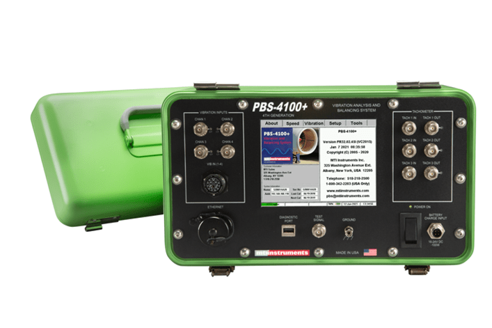
 MTI Instruments Announces Newest Addition of the PBS-4100+ Portable Vibration and Balancing System Gallery
MTI Instruments Announces Newest Addition of the PBS-4100+ Portable Vibration and Balancing System
Brand-MTI, Industry-Aerospace, Industry-Compliance Testing, Industry-Manufacturing, Industry: Transportation, New & Press Releases, News-MTI, News-MTI-PBS, News-Product Updates, News-Products, Press Releases-Vitrek, Products-MTI, Products-MTI-Engine Balancing, z1
MTI Instruments Announces Newest Addition of the PBS-4100+ Portable Vibration and Balancing System
[/fusion_builder_row][/fusion_builder_container] [/fusion_text] [/fusion_builder_column][/fusion_builder_column][/fusion_builder_column] [/fusion_builder_row][/fusion_builder_container] [/fusion_builder_column][/fusion_builder_column] [/fusion_text] [/fusion_builder_column] [/fusion_builder_column]Learn More About PBS-4100+ Gen4 [/fusion_builder_column] MTI Instruments Announces Newest Addition of the PBS-4100+ Portable Vibration and Balancing System; Continuing its Industry Leading Excellence in Aircraft Engine Maintenance Systems The fourth-generation iteration of MTI Instruments’ engine vibration analysis and balancing system is more mobile than ever, while maintaining the highest standards in the industry for commercial aviation Lockport, IL, April 27, [...]