Silicon carbide (SiC) wafers are in high demand, particularly in high-temperature applications. Silicon carbide (SiC), a semiconductor material made of both silicon and carbon, can withstand extreme temperatures of up to 2700°C. Often referred to as carborundum, SiC’s unique properties also make it a key material in non-electronic applications such as bulletproof vests, extrusion dies, sandpaper, and high-performance disc brakes.
In the electronics industry, SiC wafers are crucial for devices operating under high temperatures, high voltages, or both. For example, they are used in electric vehicle (EV) power electronics, 5G communication systems, and LED technology, making SiC a material of great interest to sectors where energy efficiency, high performance, and durability are essential.
Bandgap and Thermal Conductivity: Why SiC Wafers Are Essential for High-Voltage Applications
SiC wafers are renowned for their wide bandgap, which is 3.26 eV—significantly higher than silicon (Si) at 1.12 eV and gallium arsenide (GaAs) at 1.42 eV. This wide bandgap allows SiC wafers to withstand voltages up to ten times higher than silicon wafers. SiC’s wide bandgap also facilitates faster switching speeds, greater efficiency, and the ability to support smaller, thinner devices.
Furthermore, silicon carbide’s superior thermal conductivity enables better heat dissipation in electronic components. This reduces the need for bulky heat sinks and supports the miniaturization of devices. SiC wafers are integral to ensuring optimal performance in power electronics, such as those found in electric vehicles (EV) and 5G systems, where both high voltage and high temperature are factors.
Thermal Shock Resistance: SiC’s Resistance to Temperature Variations
Due to its high thermal conductivity and low thermal expansion, silicon carbide offers excellent resistance to thermal shock. This type of stress occurs when rapid temperature changes cause certain parts of an object to expand and contract at different rates, potentially leading to fracture. SiC’s ability to withstand such temperature fluctuations without breaking down makes it indispensable for devices that must endure harsh conditions.
Compared to other materials, SiC’s resistance to thermal shock makes it ideal for use in high-performance electronics and automotive applications, where temperature variations are common.
Physical, Chemical, and Electrical Durability of SiC Wafers
The physical durability of SiC is demonstrated by its use in tough applications like bulletproof vests. It is chemically inert and can resist aggressive chemicals, including alkalis and molten salts, even at temperatures as high as 800°C. Its ability to maintain structural integrity under extreme conditions contributes to its use in non-electronic applications as well as semiconductor devices.
SiC wafers are also highly resistant to electromagnetic interference (EMI) and radiation, making them ideal for high-energy applications where exposure to electromagnetic disturbances is a concern.
What are silicon carbide wafers used for?
Silicon carbide wafers are critical in modern electronic devices, particularly in electric vehicle (EV) power electronics. SiC’s properties support power applications that demand high efficiency, low power consumption, and compact designs. Some key SiC wafer applications include:
- On-board DC/DC converters
- Off-board DC fast chargers
- On-board battery chargers
- EV powertrains
- Automotive LED lighting
Beyond automotive applications, 5G electronics also rely on SiC wafers for their greater power density and higher heat tolerance. According to Cree Wolfspeed, gallium nitride (GaN) on SiC is poised to be the optical solution for 5G communication systems, offering faster data transmission speeds and improved performance.
Types and Grades of SiC Wafers
SiC wafers come in multiple grades, including semi-insulating and conductive types. Depending on the application, wafers are manufactured in sizes from 100 mm to 200 mm, with both 4H and 6H polytypes used for different device characteristics.
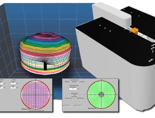
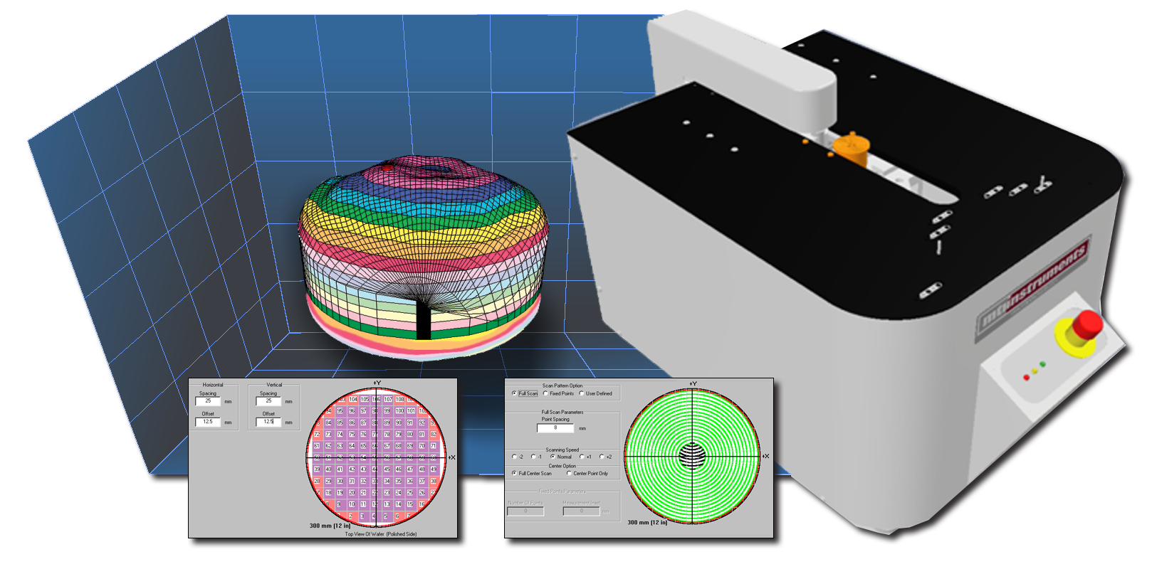
The Importance of SiC Wafer Measurement and Inspection
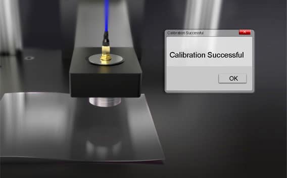
As the demand for SiC wafers continues to grow, ensuring their quality becomes increasingly important. Proper inspection equipment is vital to avoid defects in components. In research and development (R&D) phases, poor verification of process tools can drastically reduce yield and affect the performance of devices.
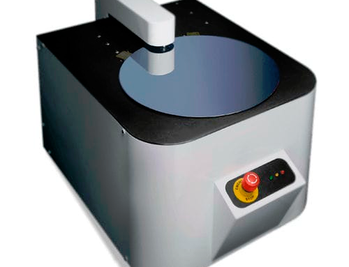
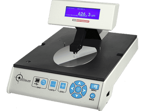
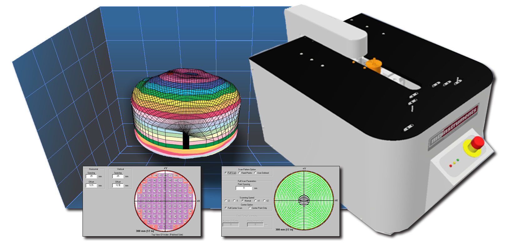
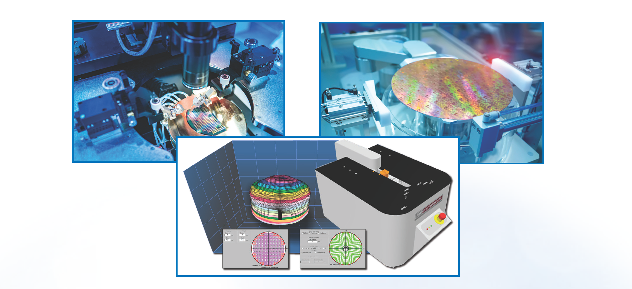
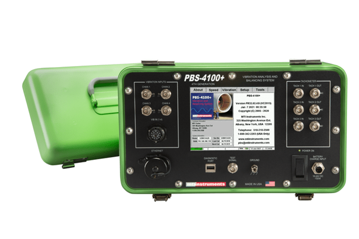
To address this, MTI Instruments offers the Proforma 300iSA system, a semi-automated measurement system that inspects SiC wafers at-scale (up to 20 wafers per hour). This system provides comprehensive scanning for thickness, total thickness variation (TTV), bow, flatness, and other critical parameters, ensuring high-quality SiC wafers for advanced applications.
The Growing Significance of SiC Wafers
Silicon carbide (SiC) wafers continue to gain momentum in industries that demand high-performance materials for high-temperature and high-voltage applications. From electric vehicles to 5G communication, SiC wafers provide the thermal conductivity, bandgap width, and durability required for cutting-edge technology. As the demand for these wafers grows, ensuring quality through precision wafer inspection is key to maximizing their potential.
To learn more about MTI’s measurement solutions for SiC wafers, or to download a sample wafer inspection report please contact MTI Instruments.


