
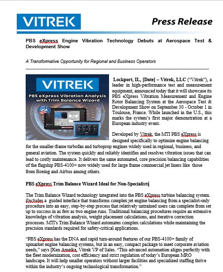
Semiconductor Wafer Measurement for Increased Productivity
This three-part article describes how manufacturers leverage capacitance-based inspection systems for semiconductor wafers. The article reviews best-practices, consequences of failing to inspect semiconductor wafers and benefits of using semi-automated, fully-automated and manual systems for wafer metrology and inspection.

Part 1: Why Disc Geometry Matters in Wafer Production
Semiconductor wafers are cut from cylindrical silicon crystals, or ingots. The flatness of these disc-shaped wafers is controlled to tight tolerances to ensure that the entire wafer surface is suitable for integrated circuit (IC) production. If disc geometry is out-of-spec after cutting, it may be possible to reprocess the wafer. Cutting is only the first step in wafer processing, however, and subsequent steps such as lapping and polishing, thin film deposition, and lithography can add costs that result in significant waste if a wafer fails to meet dimensional specifications. This article explains why disc geometry matters at each step in wafer processing – and what can go wrong.
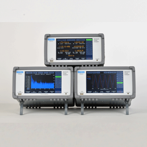
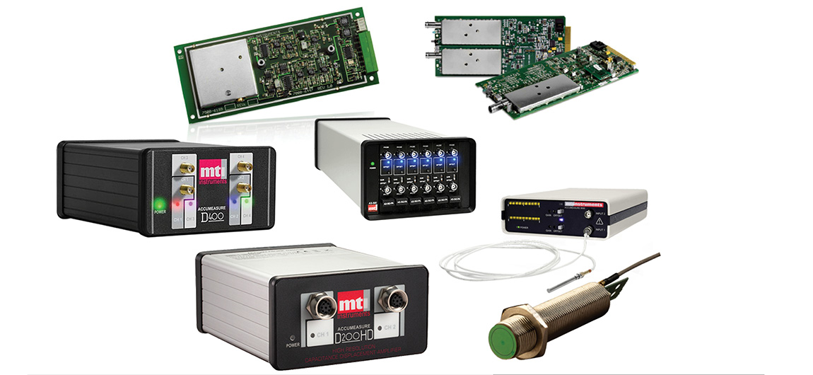
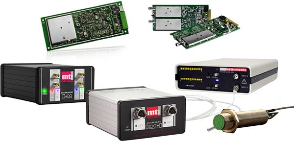
Semiconductor manufacturers choose capacitance-based inspection and metrology systems for semiconductor wafers. In the front end of the wafer processing procedure, these systems can measure disc geometry and thereby ensure that wafers, which are often valued at thousands of dollars, are suitable for additional operations. MTI’s Proforma family of products, and Digital Accumeasure technology, for example, provide inspection and measurement solutions that are fast, easy-to-use, and cost-effective. For the semiconductor industry, the benefits of using these systems include increased profitability through reduced waste and costs.

Wafer Cutting

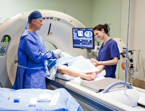
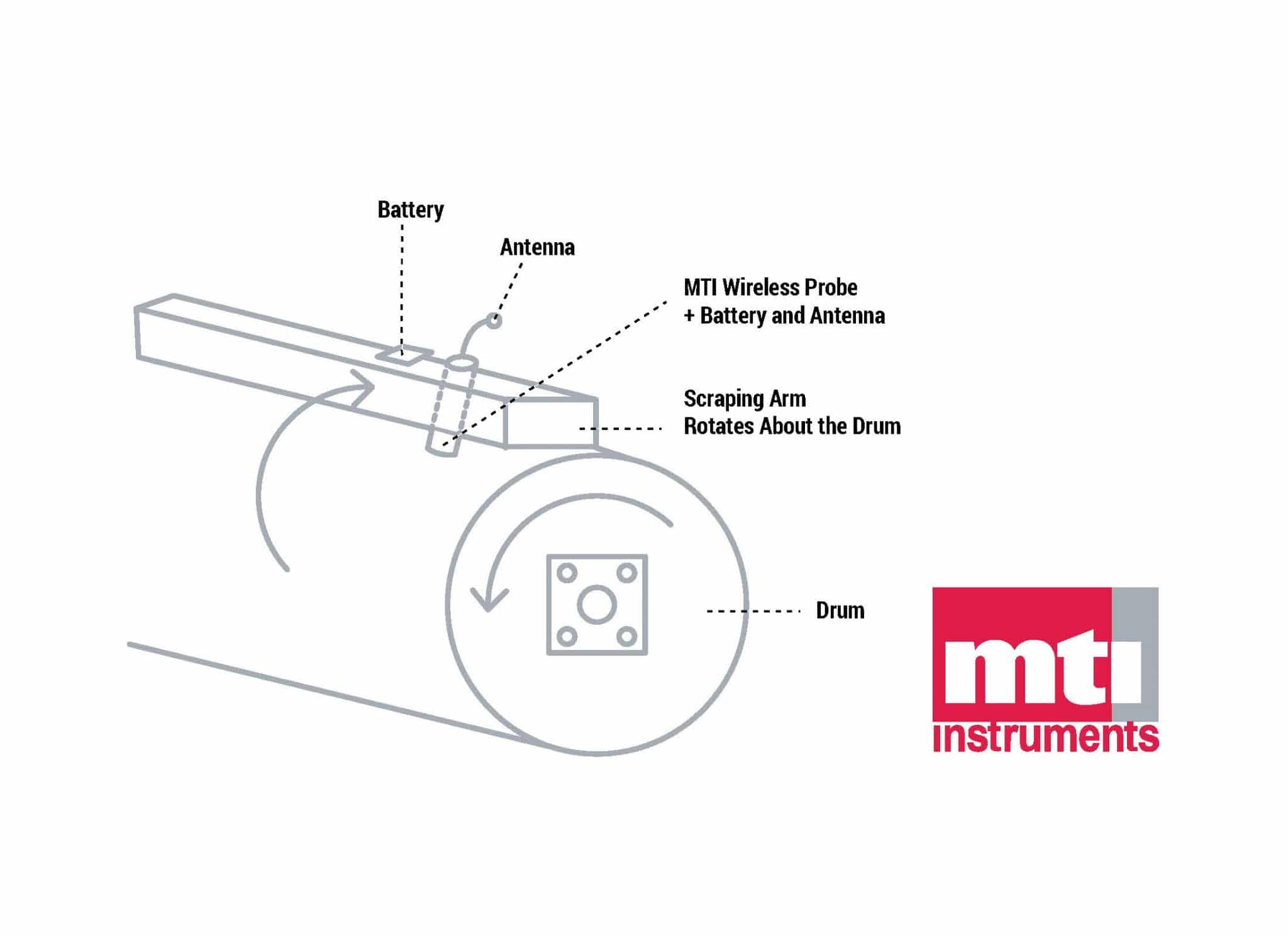
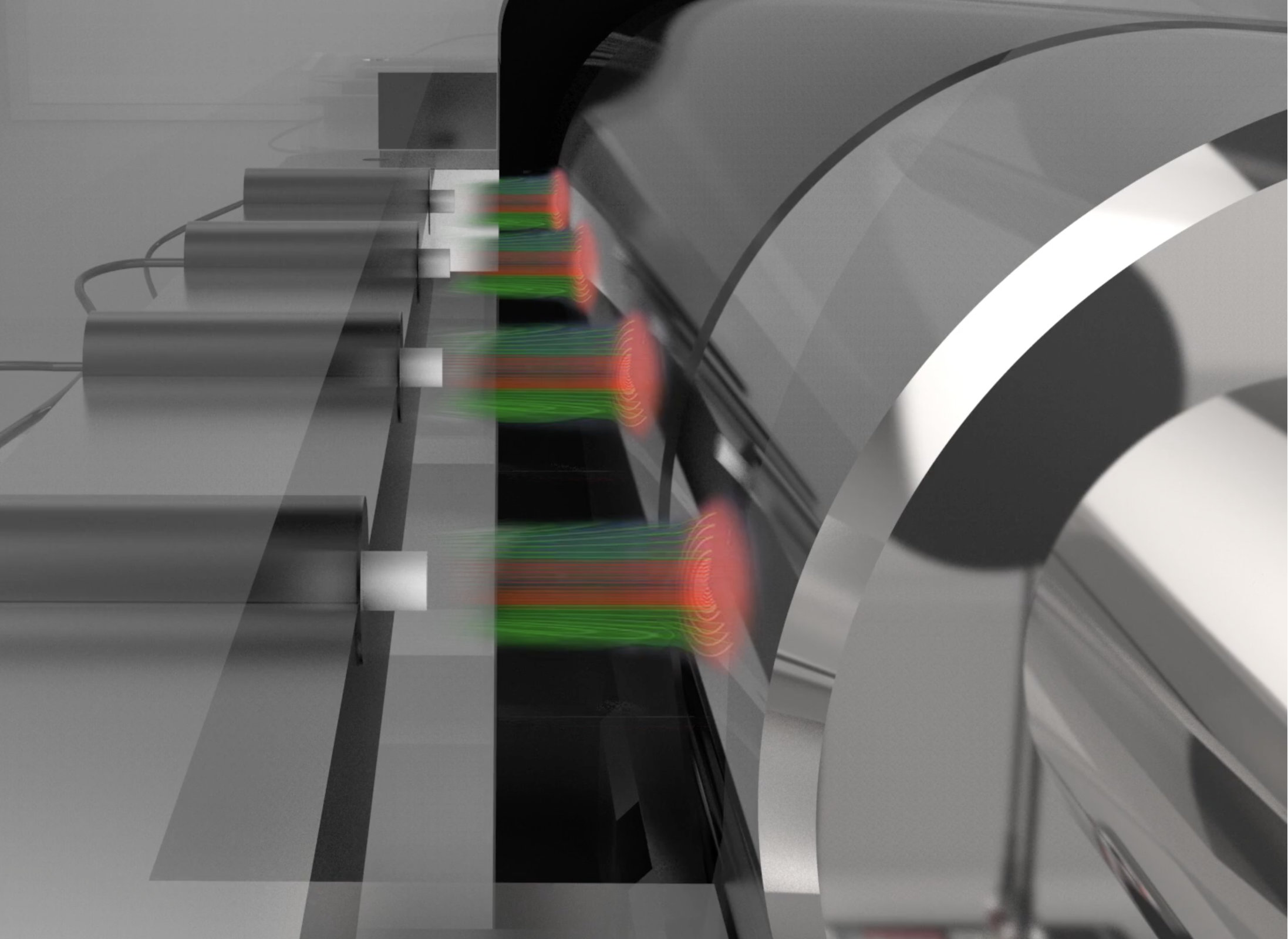
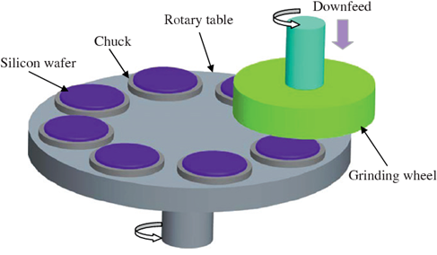
Figure 1. Rotary table for semiconductor wafer lapping.
Capacitive gap measuring probes eliminate the need for mechanical feeler gauges. Users quickly measure the gap between During wafer sawing, silicon ingots are sliced to a specific thickness. The diameter of a slice determines the diameter (e.g., 300 mm), which is typically referred to as the “size”, of the wafer. To avoid ruining the disc and creating scrap (or requiring reprocessing), wafer cutters need to use the right type of wire saw based on the thickness of the disc and the width of the “streets”, or cut lines, that separate individual dies. It’s also important to minimize heat buildups that can result in chipping or cracking, or the production of excessive dust.
There are many types of wire saws, including ones that are manual or automated, support single-wire or multi-wire cutting, cut in one or two directions, and are mounted on different sized hubs with varying spindle rotational speeds. Through proper tool selection and parameter optimization, wafer cutters can ensure that a disc’s geometry is suitable for additional processing. Manual metrology systems, such as MTI’s Proforma 300i, for example is a wafer thickness gauge and differential measurement system that provides a cost-effective alternative to full-automated systems.
Thin Film Deposition
Thin films are deposited onto wafers to impart electrical, optical, and mechanical properties that enhance semiconductor performance; however, these coatings need to have a specific thickness that is uniform across the entire wafer substrate. Irregular deposition that is too thin (or too thick) in spots may not meet performance requirements and, consequently, can result in wafer waste. Whether the deposition method is chemical or physical, it is important to measure a wafer’s thickness both before and after thin film deposition.
Capacitance-based systems provide a high level of stability, repeatability, and accuracy during inspection and measurement. For example, during the build-up of a metal oxide film, a consumable capacitance probe within the deposition chamber can measure the thickness of the dielectric material by detecting the impedance change and using a co-located ground electrode. Utilizing technologies like MTI’s Digital Accumeasure, an amplifier located outside of the chamber can convert a highly precise capacitive electric field into a highly precise 24-bit digital deposition thickness reading. This technology can also be used to measure the thickness of conductive films through pre-deposition and post-deposition thickness measurements.
Lithography
Semiconductor lithography creates ICs by transferring complex patterns of geometric shapes onto thin films. With optical lithography, or photolithography, variations in the wafer surface need to be smaller than the depth of focus of the exposure tools. Because previous wafer processing steps such as grinding, lapping and polishing can impact disc geometry, it is important to measure thickness, TTV, warp, and bow. Otherwise, the expensive manufacturing equipment that is used in semiconductor lithography can add costs that result in significant waste.
The reticle, or photomask, in optical lithography is the master template for an IC design. If the reticle is not co-planar with the wafer, poor exposure and defective ICs may result. Traditionally, lithography companies used capacitance probes to keep the reticle co-planar with the wafer; however, optical sensors are now used instead because they can achieve a larger standoff distance. If stand-off is not an issue, capacitance still provides a fast, cost-effective, and relatively easy-to-use measurement technology. Capacitance probes are stable, precise, and capable of nanometer resolution.
Part 2: The Cost of Failing to Inspect Semiconductor Wafers
Most semiconductor wafers are made of silicon, the second most common element in the Earth’s crust. Yet, silicon’s abundance does not mean that wafers are inexpensive. The pure form of silicon that’s used in semiconductors does not occur naturally and must be refined and mixed with a dopant that alters material properties and electrical characteristics. Silicon ingots are formed, wafers are cut, and more costs are added during subsequent processing steps that include lapping and polishing, thin film deposition, and lithography. This article, the second in a series, considers the costs associated with wafer fabrication and explains why it’s worth inspecting and measuring wafers during each processing step.
Inspection and metrology systems are available for semiconductor wafers made of silicon, silicon carbide (SiC), germanium (Ge), indium phosphate (InP), and gallium arsenide (GaAS). Manual and semi-automated systems make non-contact measurements of disc geometry, the subject of Part 1 of this whitepaper. Because capacitance-based systems cost significantly less than equipment that is fully automated, semi-automated and manual solutions provide a faster return on investment (ROI). Moreover, manual and semi-automated inspection and metrology systems can be used at the front end of processing before significant costs are added with lithography. By that point, the amount of waste can be in the thousands of dollars.
The High Cost of Wafer Waste
With each processing step, the costs associated with a wafer increase. According to Wafer Pro, bare discs can range from $27 to $98 (USD). According to Wafer World, $100 to $500 per disc is typical since prime grade wafers cost significantly more than test grade, dummy grade, or reclaimed wafers. Finished semiconductor wafers that combine high performance with high density are even more valuable. As reported by the website Tom’s Hardware, TSMC’s estimated price for a 300 mm wafer at 5 nm is nearly $17,000. In part, that’s because the new N5 technology that TSMC uses to produce these wafers requires significant capital expenditures (CapEx).
The Tom’s Hardware estimate far exceeds the approximately $9500 that TSMC charges for a 300 mm wafer patterned with N7 technology. The company also sells 300 mm wafers at 16 nm or 12 nm for about $4,000. Regardless of their sales price, any of these finished wafers has incurred much greater costs than a cut and polished disc. Whether it’s for older designs that use existing manufacturing technologies or newer wafers made with next-generation nodes, the semiconductor industry risks adding expensive waste by failing to inspect wafers before subsequent processing occurs. Simply put, it’s better to discard a $100 bare disc than a $4,000, $9,500, or $17,000 finished wafer that’s been patterned and packaged.
Disc Sizes, Fabrication Costs and Rates of Increase
Because CapEx takes years to depreciate, the cost per square inch of silicon is at its highest whenever a new wafer size is introduced. Costs per square inch decrease over time, but there are also higher fabrication costs with larger wafer diameters. In an article for SEMI called The Macroeconomics of 450 mm Wafers, Apek Mulay writes that “for every succeeding increase in wafer size, there is approximately a 1.4 increase in costs of manufacturing.” Therefore, companies that process wafers in the world’s most popular size, 300 mm, already have higher fab costs than processors of 125 mm or 200 mm discs.
For wafers in all sizes, the semiconductor industry can also expect to pay higher fabrication costs over time. In a report from the Center for Security and Emerging Technology (CSET), authors Saif M. Khan and Alexander Mann write that “the highest-value sectors”, which include semiconductor fabrication, “have seen especially steep rates of cost growth”. Since the early 2000s, fab costs have risen at over 10% per year. The CSEET report, AI Chips: What They Are and Why They Matter, also warns that “as semiconductor complexity increases, demands for high-end talent drives fabrication cost overruns”. Fixed costs pose high barriers to entering the industry, but variable costs are squeezing the profits of existing players.
Part 3: The Benefits of Manual, Semi-Automated, and Fully Automated Systems for Semiconductor Wafer Inspection & Metrology
Fully automated systems that can load, scan, and unload wafers are fast, convenient, and efficient at high volumes. They’re useful for checking every wafer in every batch, but these systems are expensive. Semi-automated and manual systems cost significantly less and are generally used for lower volumes; however, they’re also easy-to-use and can make fast, accurate measurements that support production flow. Semi-automated and manual systems also support spot testing, or wafer sampling, in a batch.
Within the semiconductor industry, there are applications for each type of system. For example, fully automated systems may be required for inspecting and measuring critical, high-value central processing units (CPUs) where a manufacturer wants to check every wafer. For less complex microelectronics, or for less valuable integrated circuits (ICs), a manufacturer may decide that it’s more cost effective to sample representative wafers instead. There are also ICs, or discrete components, where line widths are large and the maximum focal plane deviation, a measure of flatness, is less critical. With applications like these, a manual or semi-automated system can provide a cost-effective solution.
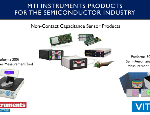
Capacitance-Based Technology for Non-Contact Wafer Inspection
MTI Instruments of Lockport, IL (USA), for example, makes manual and semi-automated non-contact wafer inspection and metrology systems that are  capacitance-based. These systems can evaluate a thousand points per minute by measuring the ratio of change in an electric charge to the corresponding change in the electrical potential (i.e., voltage). MTI’s capacitance-based systems are also faster and more precise than more expensive optical systems that use a laser or beam of light.
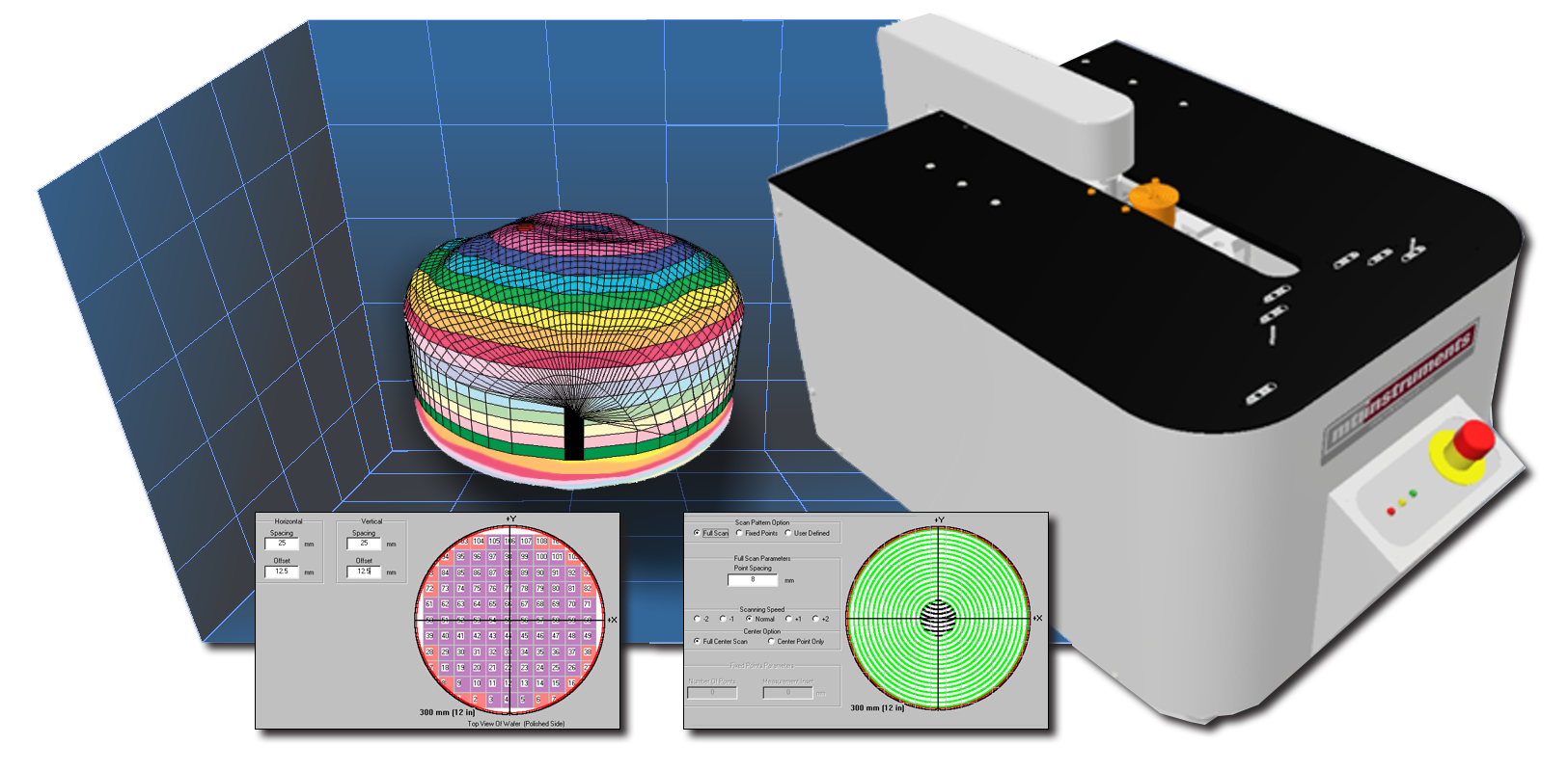
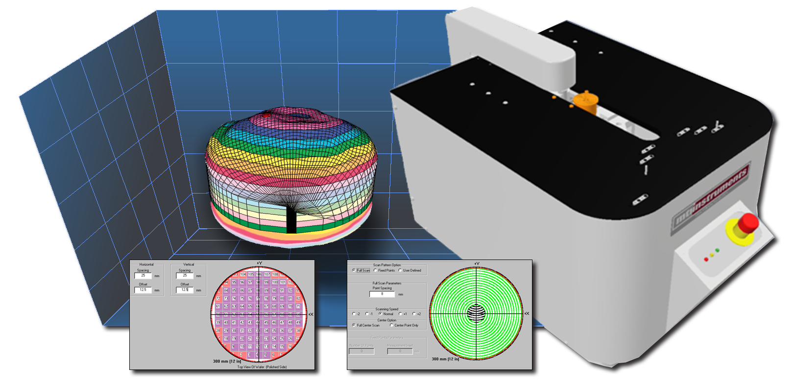
MTI’s Proforma technology uses two high-resolution non-contact capacitive probes to measure the distance from the probe to the wafer under test. One probe is on top and the other is under the wafer to measure the differential thickness. Because the probe’s sensing elements also provide some spatial averaging, this arrangement also works well with as-cut or unpolished wafers.
Proforma Technology for Non-Contact Wafer Inspection
 MTI’s proprietary push-pull™ probes do not require the wafer to be grounded. The probes also only measure to the surface of the wafer and are not affected by subsurface resistive or optical properties (i.e., transparency effects, such as with SiC). Proforma systems can measure wafers up to 300 mm and in a wide range of disc sizes, thicknesses, and semiconductor material types.
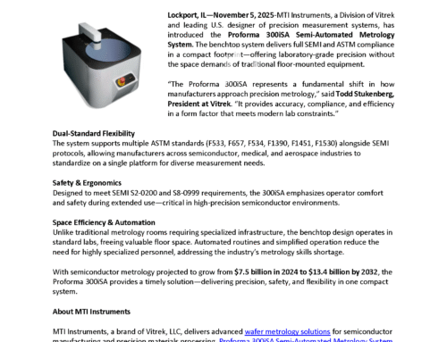
The Proforma family of products includes two solutions for the semiconductor industry. Applications include qualifying new materials, quality control (QC), quality assurance (QA), and wafer sampling.
- The Proforma 300i is a manual metrology and inspection system that is a wafer thickness gauge and a differential measurement system that also measures bow.
- The Proforma 300iSA is a semi-automatic system that provides full wafer surface scanning; delivers a more robust set of measurements, including both bow and warp; and supports stress analysis testing.
The Proforma 300i Manual Semiconductor Metrology System
The Proforma 300i is a cost-effective choice for applications where a manufacturer needs a wafer thickness measurement. This manual system does not provide full-surface wafer scanning. Instead, it provides a point-based measurement from where the operator places a wafer between two fixed probes with a known fixed gap. The Proforma 300i measures wafers from 76 to 300 mm, has a measurement range up to 1700 μm, with an accuracy of ±0.25 μm. It can be used with the following types of semiconductor materials.
- Silicon (Si)
- gallium arsenide (GaAs)
- germanium (Ge)
- indium phosphate (InP)
- silicon nitride (SiN)
- silicon carbide (SiC)
In addition to measuring substrate thickness, the system can measure five-point total thickness variation (TTV), the minimum and maximum thickness on the wafer. An optional feature, a bow wafer ring, allows for the measurement of bow, the deviation of the center point of the median surface of a free, un-clamped wafer from the reference plane.
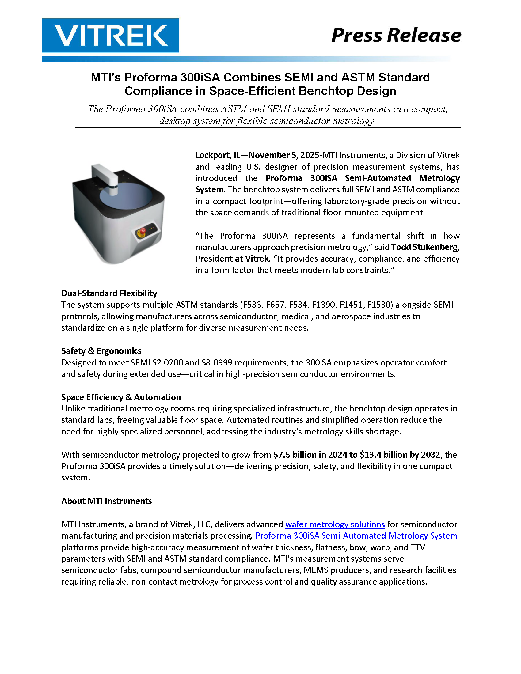
The Proforma 300iSA Semi-Automated Metrology System
The Proforma 300iSA measures wafer thickness, TTV, and bow along with warp, site flatness, and global flatness. It also supports the use of parameters for comparative purposes and the indication of whether a wafer is out-of-specification. By looking at the entire median surface of the wafer instead of just the position at the center point, warp provides a more useful measurement of the true wafer shape. Flatness measurements are important to ensure that the wafer is suitable for lithographic processing. Otherwise, defective IC patterns can raise costs through waste.
The Proforma 300iSA has a measurement range of 100 to 1700 μm and an accuracy of ±0.25 μm. This semi-automated system can be used with the same materials as the Proforma 300i, including silicon carbide (SiC), an increasingly popular choice for applications such as the power electronics in electric vehicles (EVs). The Proforma 300iSA has up to a 1700 μm thickness range & can measure wafers with the following diameters:
- 76 mm
- 100 mm
- 125 mm
- 150 mm
- 200 mm
- 300 mm
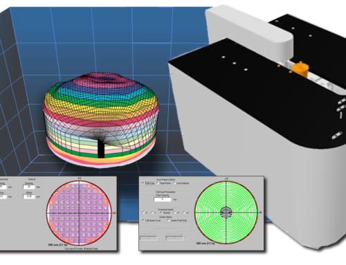
Because semi-automated systems deliver full wafer surface scanning, it uses coordinates to indicate the region under inspection. Users can focus on a single quadrant or multiple quadrants, include or exclude the wafer’s edges or center, and also examine a defined number of points. The Proforma 300iSA, for example, can capture up to 1000 points per minute and can also output raw data for processing with other software for calculations and statistical analysis.
Finally, the Proforma 300iSA supports stress analysis for wafer characterization. During wafer processing, mechanical alterations can cause deformities that render the wafer unusable or out-of-specification. The system includes software for analyzing a wafer before and after processing to evaluate how its shape has changed. A thin film stress measurement calculation algorithm is also included. In the Analysis Area of the software, the user needs to know the semiconductor’s elasticity constant. Typically, this information is provided by the semiconductor supplier.
Metrology System Selection
MTI Instruments can help you to decide whether the Proforma 300i or the Proforma 300iSA is the right choice for your specific semiconductor wafer inspection and metrology application. Our team of experts have deep experience serving the semiconductor industry. For more information, contact us at MTISales@Vitrek.com, call (518) 218-2550 or visit us online www.Vitrek.com.


