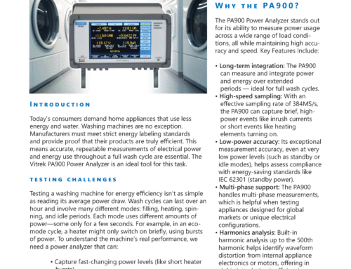
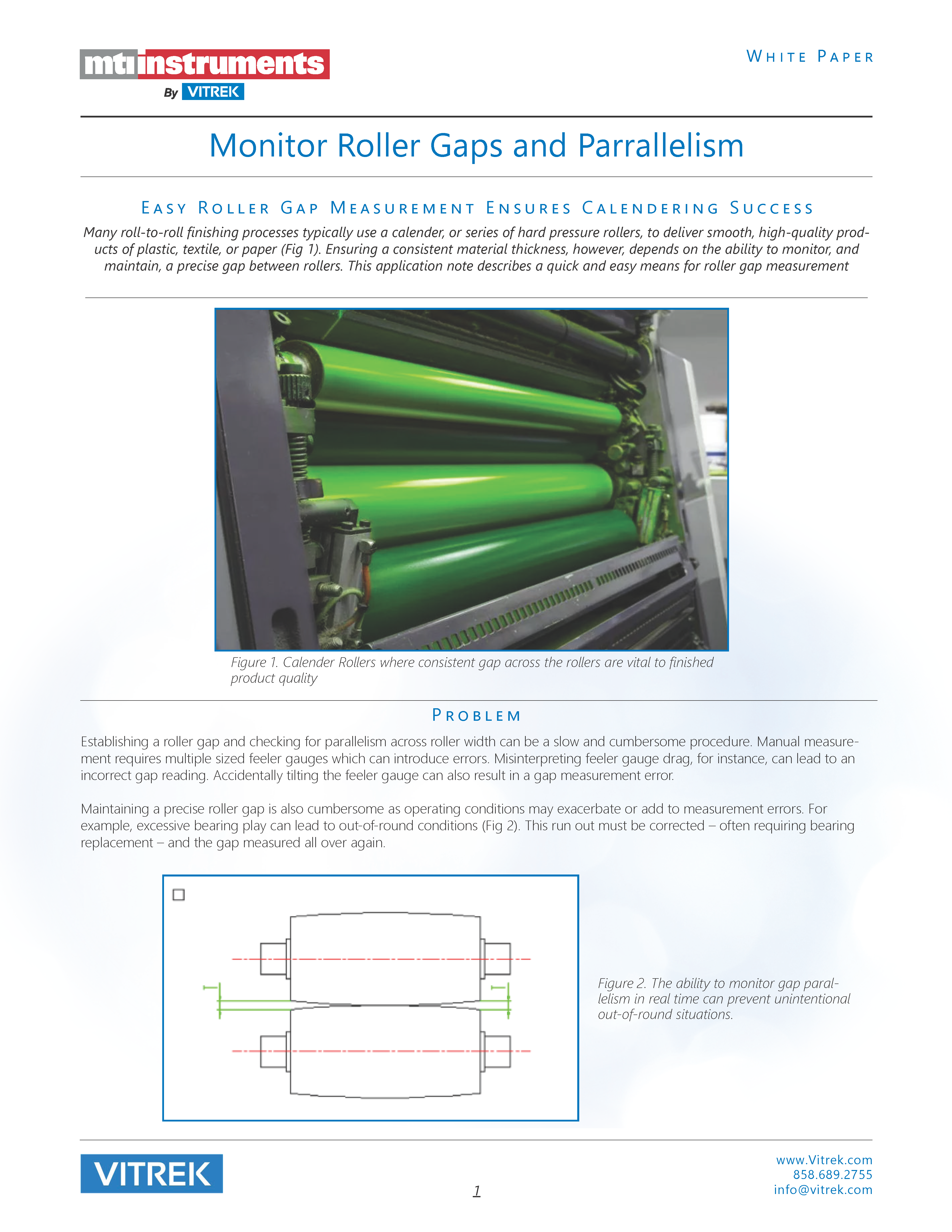
Compare silicon carbide vs. silicon for electric vehicle (EV) power electronics and learn about SiC wafer measurement.
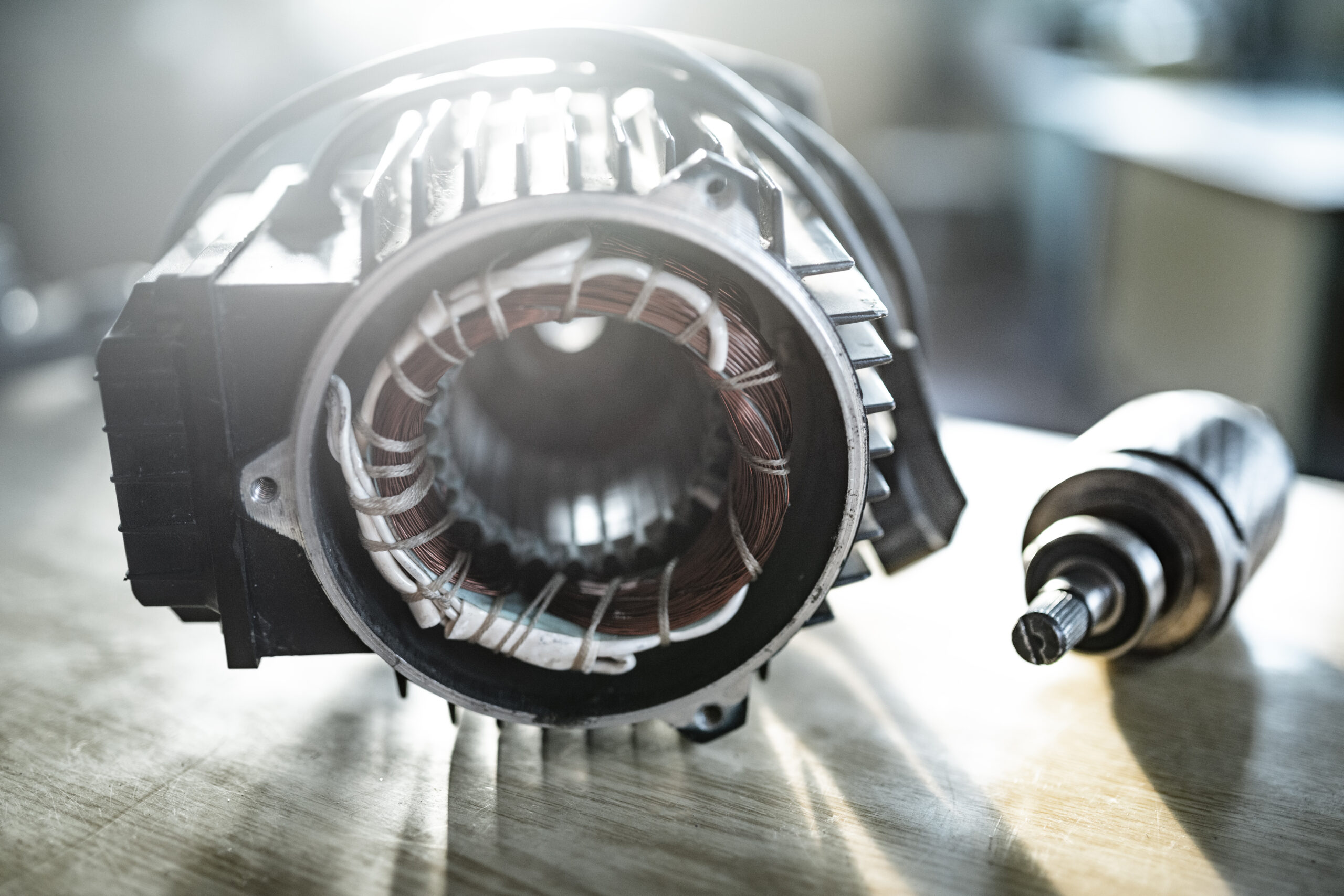
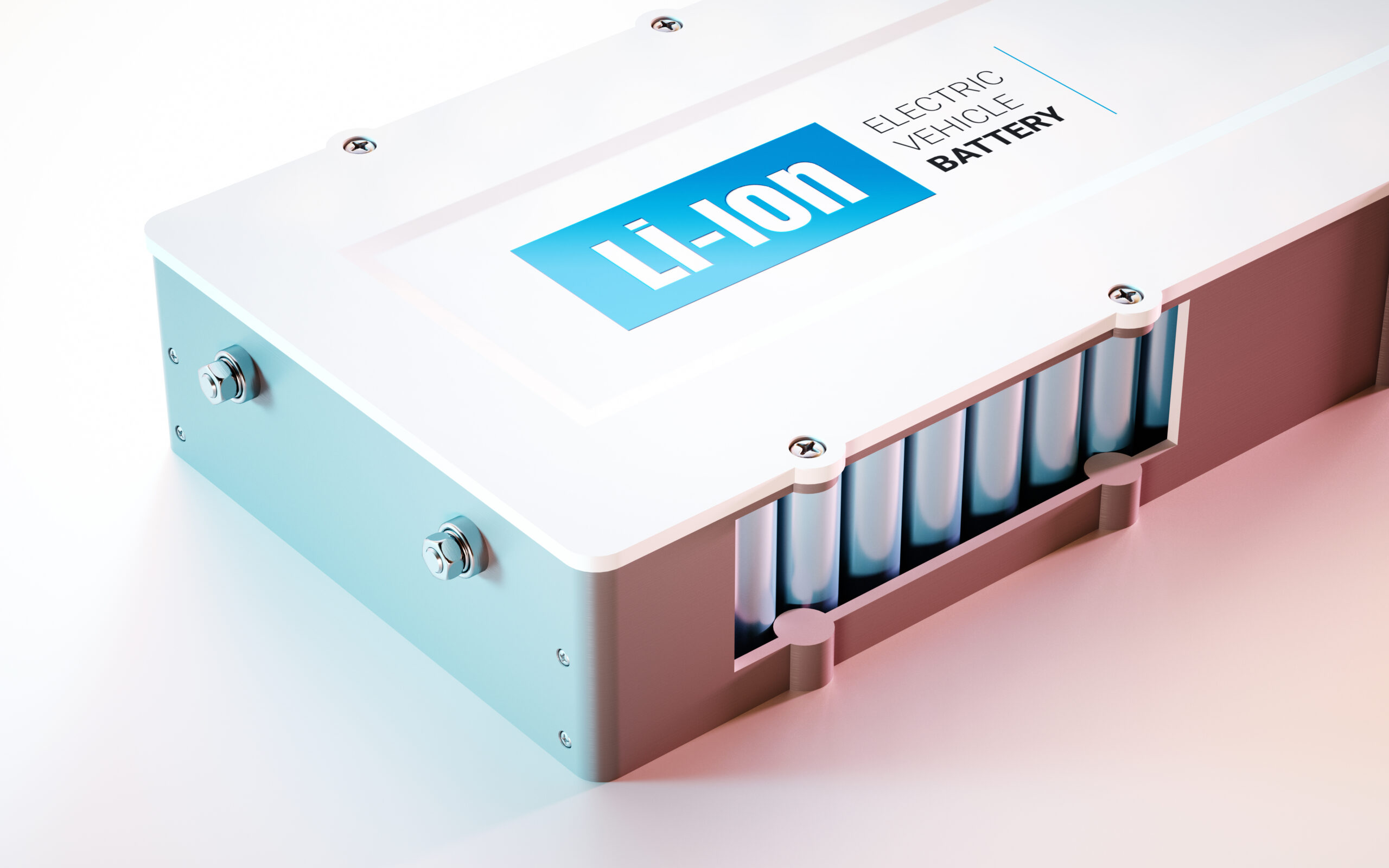
As demand for electric vehicles (EVs) continues to grow, manufacturers are comparing two semiconductor technologies, silicon carbide and silicon, for power electronics applications. Silicon carbide (SiC) provides the high temperature resistance, low power consumption, rigidity, and support for smaller, thinner designs that EV power electronics need. Examples of SiC’s current applications include on-board DC/DC converters, off-board DC fast chargers, on-board battery chargers, EV powertrains, and automotive lighting for LEDs.
According to Automotive World, SiC technology could also drive future EV innovations as battery and motor manufacturers reach the physical limits of existing technologies and need to develop more efficient drivetrains. In an interview with Semiconductor Engineering, Cree CTO John Palmour compares silicon carbide to silicon in way that the EV industry, and especially engineers, can appreciate. “You can make the device in silicon carbide that you really wanted in silicon, but due to the physics of silicon isn’t practical in that voltage range.”
The Importance of Bandgap
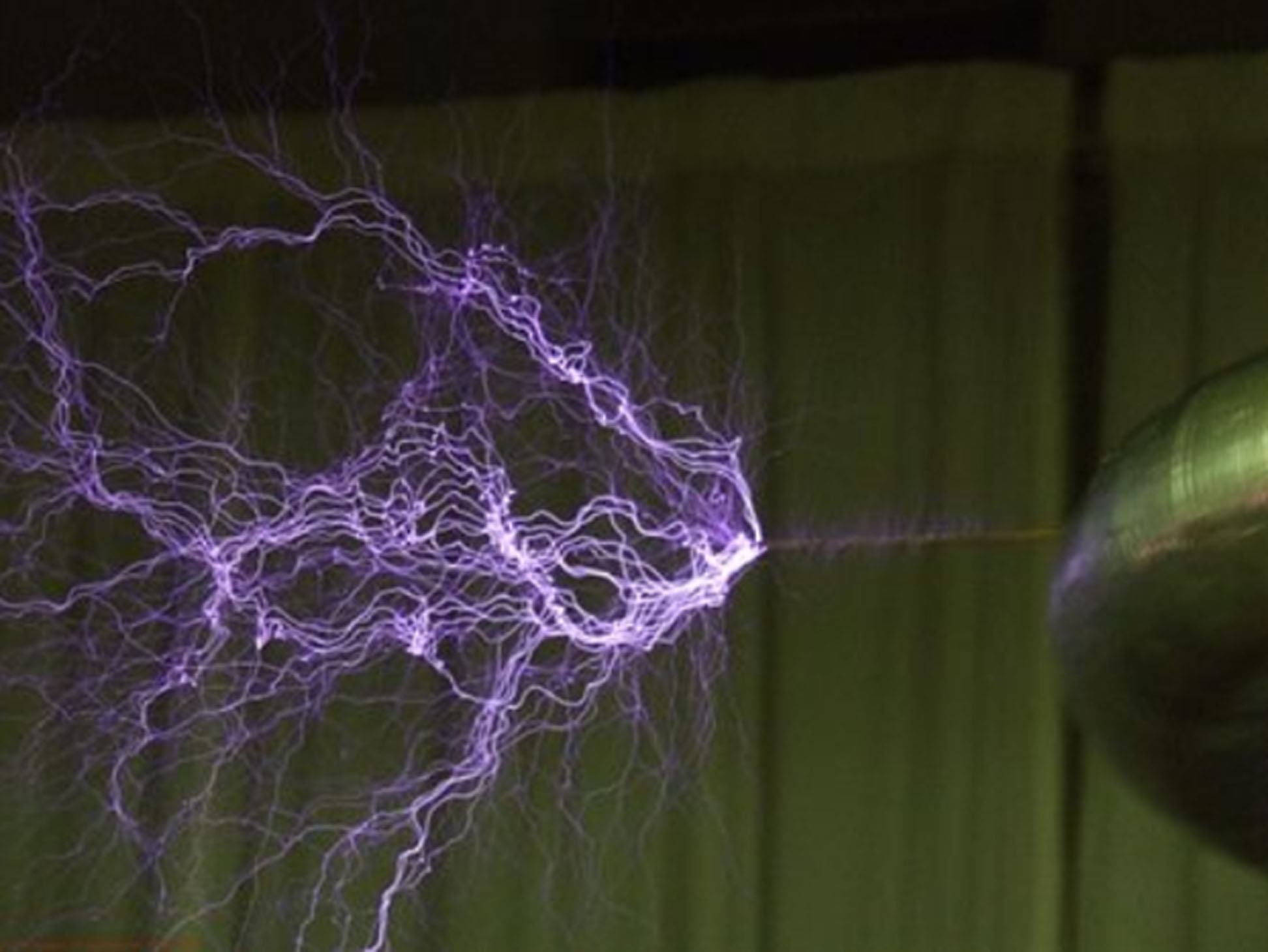
Silicon carbide’s usefulness in EV applications and other power electronics is largely a function of its wide bandgap, which is measured in electron volts (eV) and describes the energy needed to excite electrons from a material’s valence band into its conduction band. Silicon (Si), a semiconductor that’s long been the material of choice for the wafers used in integrated circuits (ICs) and photovoltaics, has a bandgap of 1.12 eV. Gallium arsenide (GaAs), a semiconductor that’s used in solar cells, has a bandgap of 1.42 eV. By contrast, silicon carbide has a significantly wider bandgap of 3.26 eV.
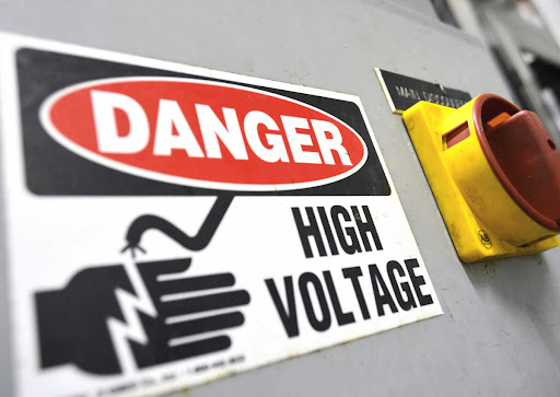
With this wider bandgap, silicon carbide is better suited for higher-power applications and the higher temperatures associated with them. Bandgap is related to breakdown voltage, the point at which a portion of the insulator becomes electrically conductive. Silicon has a breakdown voltage of around 600V, but SiC-based devices can withstand voltages that are up to ten times higher. Because bandgap shrinks as temperature rises, wider bandgap materials can also withstand much higher temperatures. Silicon carbide’s rigidity also provides a stable structure that will not expand or contract due to heat.
The wider bandgap of silicon carbide also supports faster, more efficient switching and smaller, thinner devices. Because the voltage difference, or electric potential difference, of silicon carbide does not need to be spread across as much material, SiC devices can be less than a tenth of the thickness of Si devices. These faster, thinner solutions have less resistance so that less energy is lost to heat for greater efficiency. In addition, silicon carbide’s higher thermal conductivity allows for the more efficient transportation of heat and can reduce or eliminate the need for heat sinks.
SiC Devices for EV Power Electronics: Advantages and Challenges
As reported in IEEE Spectrum, Cree estimates that the global market for silicon carbide devices topped $100 million (USD) for the first time last year. Today, the company’s SiC solutions are supporting various high voltage, high temperature components in the growing market for electric vehicles. Because an EV’s different systems are powered by different voltages, some Si devices also need to convert and portion out the correct voltages to window lifts, lighting, propulsion, and HVAC. Compared to Si devices, SiC technology supports these functions with greater speed, reliability, and efficiency.
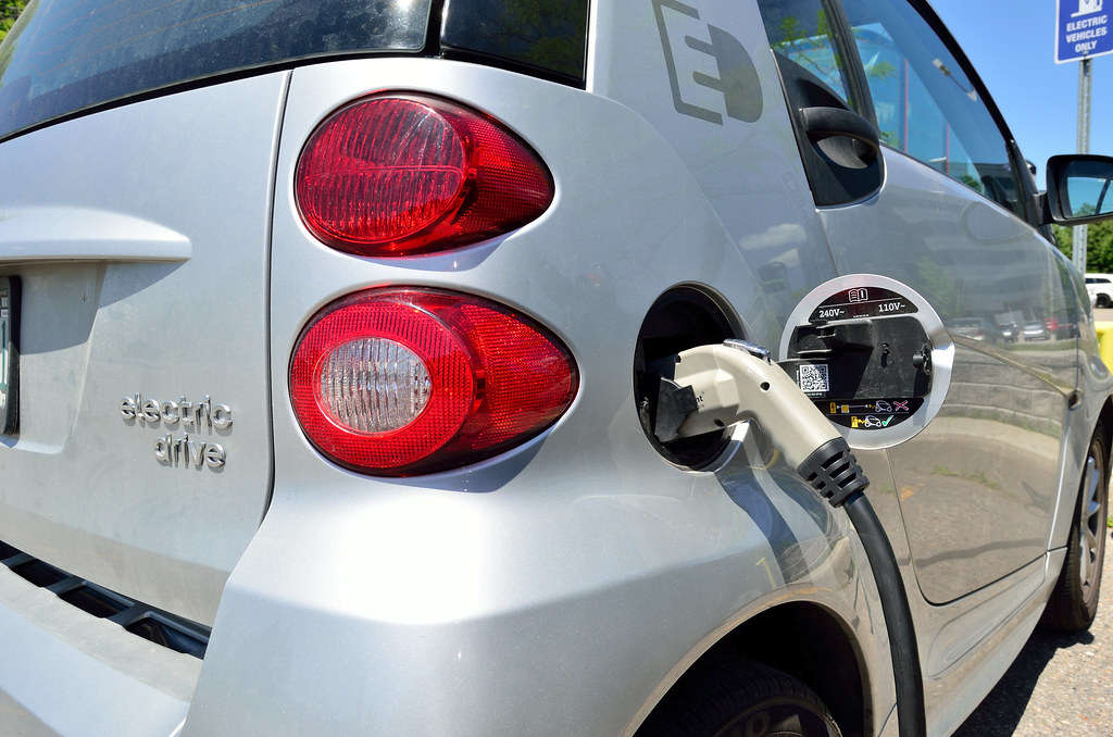
Silicon carbide’s superior switching speeds are also supporting the development of faster chargers. Off-board chargers convert incoming AC into DC for battery storage. On-board battery chargers convert DC power from the battery into AC for the main drive motor. Silicon carbide performs these functions more quickly than silicon and with less heat and energy loss. Plus, silicon carbide components can be half the size (or smaller) than silicon devices. As SiC manufacturers continue to reduce defects in the material, the prices for SiC devices are expected to decline – an advantage for future EV applications.
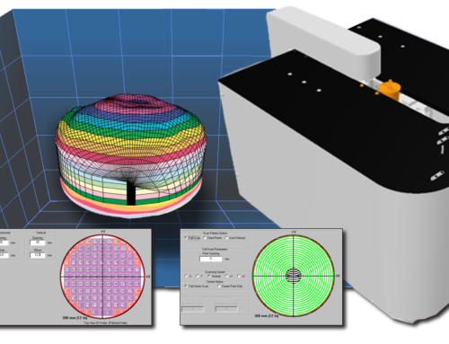
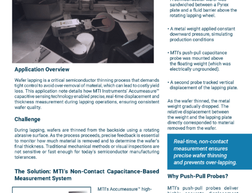
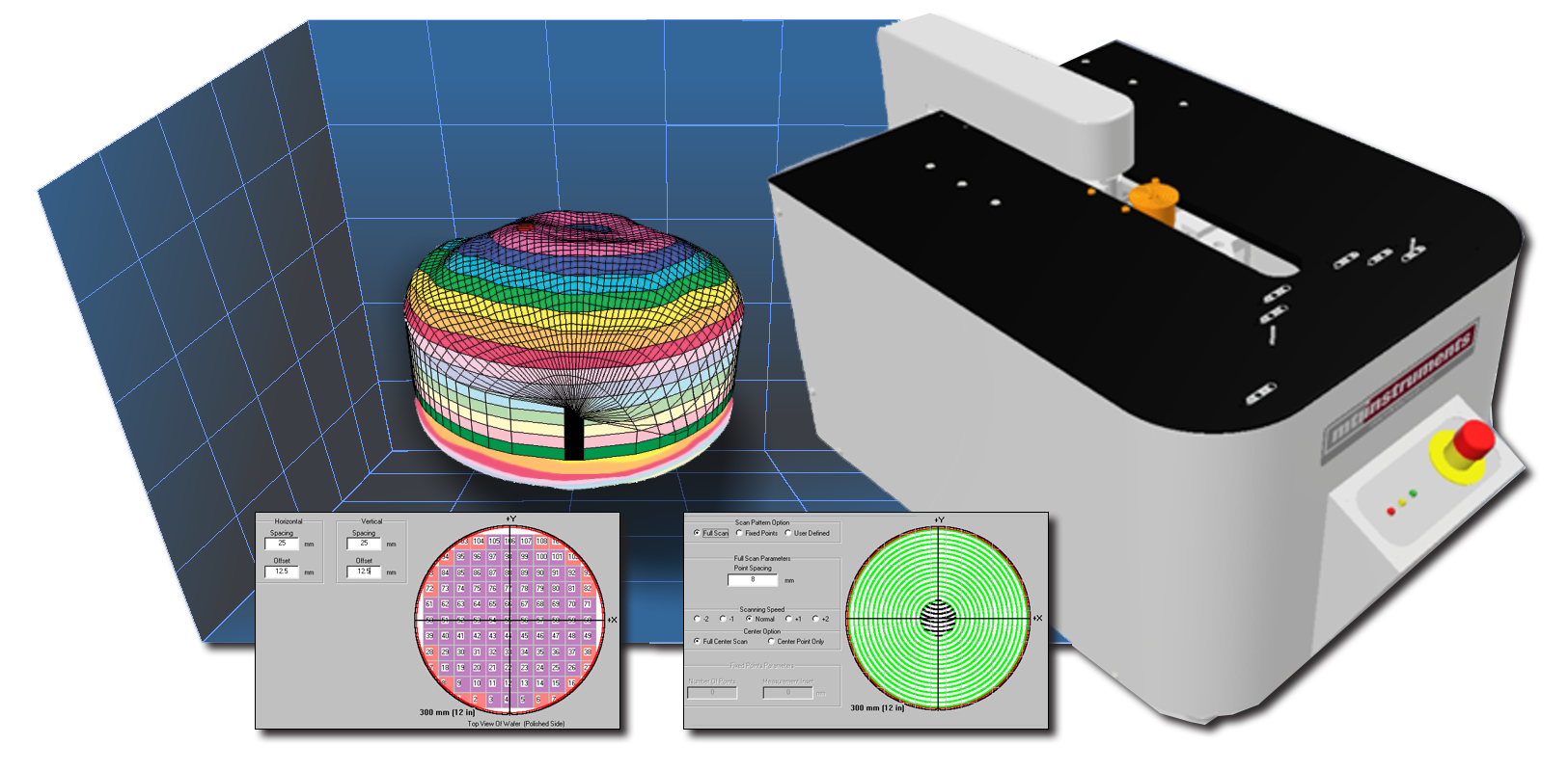
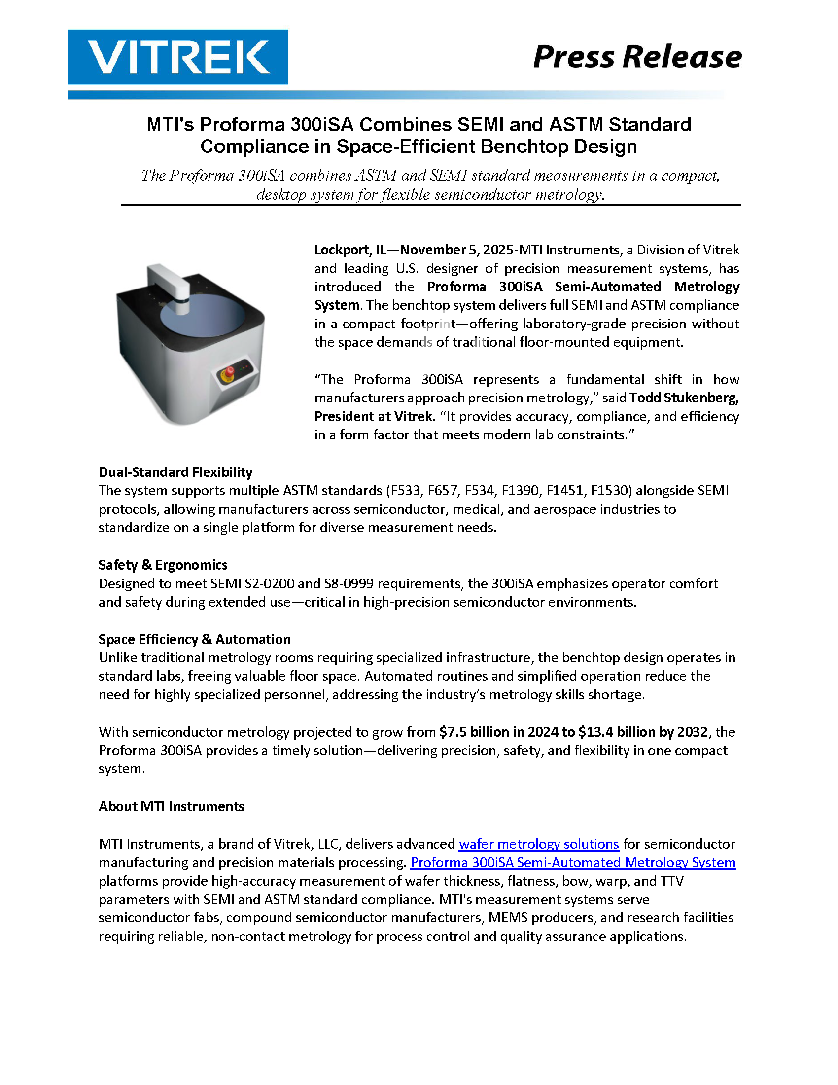
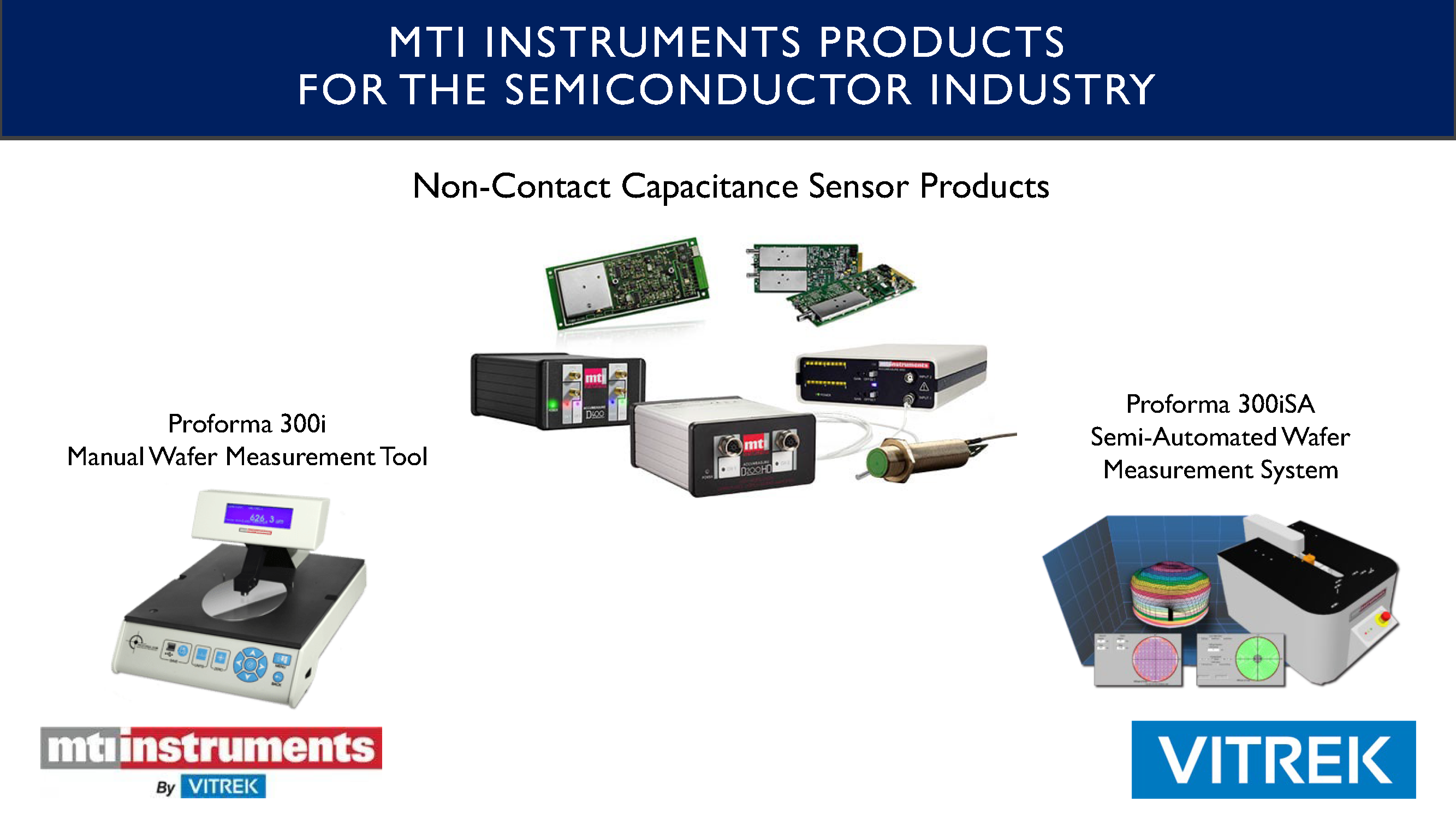
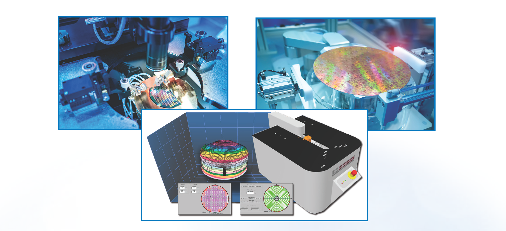
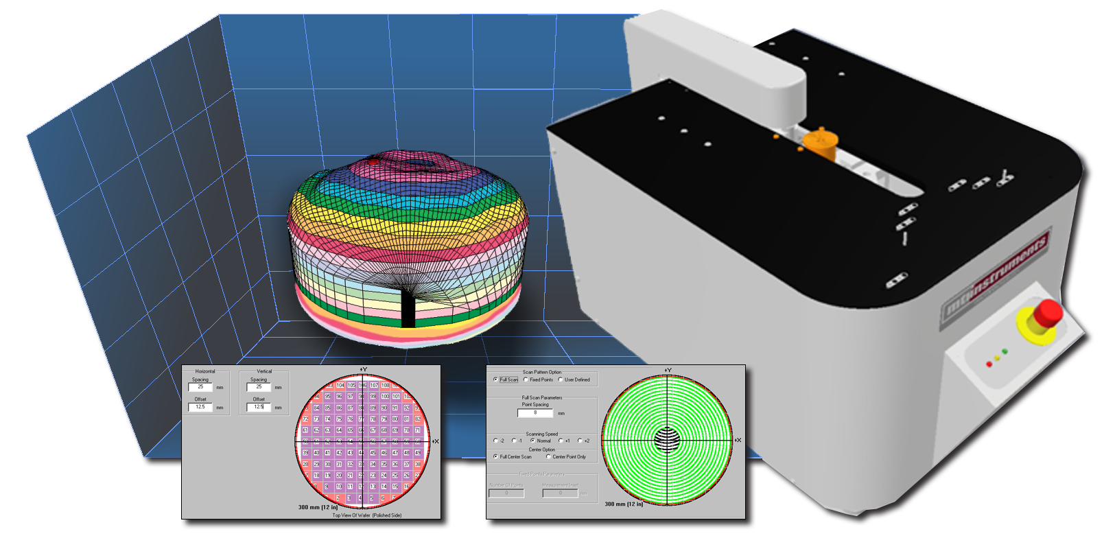
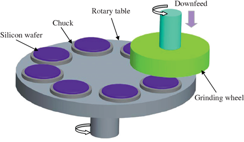
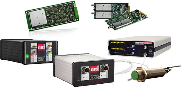
Silicon carbide’s EV prospects are bright, but increased demand for electric vehicles could result in component defects unless manufacturers install the proper inspection equipment. This is especially important during research and development (R&D), where poor verification of process tools can dramatically reduce yield. MTI Instruments’ Proforma 300iSA system performs wafer inspection at-scale and increases the throughput of SiC materials. Finding defects at volume can be difficult, but MTI’s capacitance based technology provides important advantages over confocal systems.
Capacitance Based Technology vs. Confocal Systems
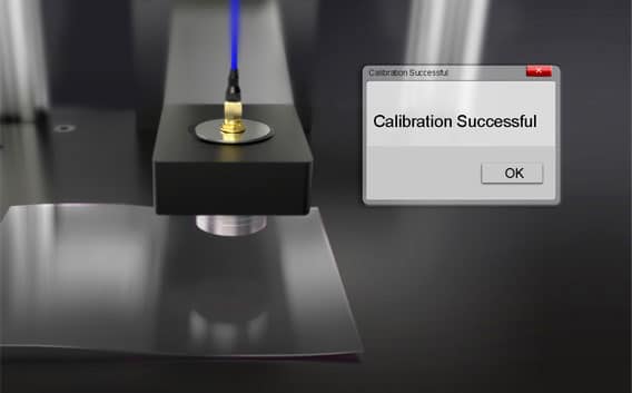
For example, high-resolution confocal interferometers cost significantly more than capacitance gauges. Laser interferometers also provide relative readings that require an operator to calibrate the instrument to a known thickness before use. By contrast, capacitance-based technologies provide absolute measurements. Plus, if a laser interferometer loses track of the wafer’s surface, the resulting measurement is inaccurate. With confocal systems, measuring transparent or translucent semiconductor wafers is more challenging, too.
Capacitive based systems provide other advantages as well. Over time, the laser sensors in confocal systems have a tendency to drift respective to temperature, thermal heating, and other factors. By contrast, capacitance circuits tend to be more stable and combine low drift with high accuracy. Capacitance based technologies like MTI’s Proforma technology can also expand the applications for quality control across the semiconductor supply chain. Vendors that sell SiC wafers can perform high-resolution measurements before shipping and can then measure SiC wafers upon receipt.
MTI Instruments ProForma 300iSA is a capacitance-based off-line measurement tool that costs less, supports quality checks earlier in the manufacturing process, and can measure wafer thickness, bow and warp, total thickness variation (TTV), and center thickness with an accuracy of ±0.25µm and a resolution of 0.05 um. In addition to supporting R&D projects, the ProForma 300iSA can be used to calibrate in-line equipment. To increase your productivity yields for the SiC wafers used in EV power electronics, learn more and ask MTI for a sample report.


