 White Paper: Precision Power Analyzers Gallery
White Paper: Precision Power Analyzers
Brand-Vitrek, Industry-Compliance Testing, Industry-Consumer Products, Industry-Electronics, Industry-Energy, Industry-Manufacturing, Industry-R&D, News-Product Updates, News-Products, News-Vitrek, Products-Vitrek-Power-Analyzer, Whitepapers-Vitrek, z1
White Paper: Precision Power Analyzers
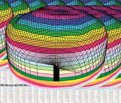
White Paper All the tools needed to study and optimize virtually any power project in a single instrument Introduction The design of any power conversion system requires the measurement of a large range of electrical parameters that could be made using a lab bench full of instruments. The precision power analyzer pulls all of these measurements into a single instrument replacing meters, oscilloscopes, chart recorders, harmonic analyzers and other devices. This paper will provide a basic overview of the functions and capabilities of high-performance power analyzers. Examples of these functions and how to apply [...]

How to Reduce Inconsistent Wafer Measurements
How to Reduce Inconsistent Wafer Measurements Avoid 5 Common Mistakes That Destroy Wafer Measurement Accuracy You take pride in your work. You’re precise, accurate and depend on the right metrology equipment. Then why are your bare semi-conductor wafer measurements sometimes inconsistent? It may be something you’re doing (or not doing) — without realizing it. MTI Instruments discovered there are five common mistakes that engineers and users make with bare semi-conductor wafers. The “Five Mistakes Made When Taking Semiconductor Wafer Measurements” Tech-Brief details these all-too-typical errors that adversely impact measurements. [...]

Vitrek featured in Bodo’s Power Systems
Click here to Download a copy of this article! Click here to Download a copy of this article!
 Five Common Mistakes with Semiconductor Wafer Measurement Gallery
Five Common Mistakes with Semiconductor Wafer Measurement
Application Notes-MTI, Brand-MTI, Industry-Compliance Testing, Industry-Consumer Products, Industry-Electronics, Industry-Manufacturing, Industry-Semiconductor, Industry-Semiconductor-MTI, Z-REPUB, z1

Five Common Mistakes with Semiconductor Wafer Measurement
Semiconductor wafer measurement requires a high degree of precision. The right metrology equipment and inspection processes are important, but so is procedural consistency and attention to detail. If you’re not getting the results you want, it’s time to look beyond the measurements. With bare semiconductor wafers, users need to avoid these five common mistakes. Mistake #1 | Turning the Device Off Most users turn on metrology devices only when it’s time to use them. As soon as semiconductor wafer measurement is complete, the devices are turned off. This reduces electricity consumption but also introduces thermal instability that can cause [...]
How to Implement a Complete Digital Closed Loop Control System
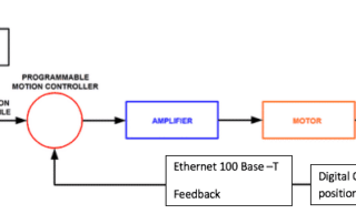
Co-authored by Don Welch, Director of Engineering and Business Development Cory Bufi, Software Engineer Isaac Abbott,Product Innovation Engineer – PBS Group Request Whitepaper Today’s electronic designs often call for reasonably fast and precise positioning of miniature components for process deposition elements such as ink jet nozzles, 3D printing elements etc. And as process control moves from mm positioning to micron to sub-micron positioning it becomes necessary to monitor and control positioning actuators such as piezo flexure stage and voice coil motors. Open loop control of the positioning stage may have been adequate in non-precision applications but piezo electric [...]
 Proforma 300i SA Video Shows Semiconductor Metrology Gallery
Proforma 300i SA Video Shows Semiconductor Metrology
Brand-MTI, Industry-Compliance Testing, Industry-Consumer Products, Industry-Electronics, Industry-Manufacturing, Industry-R&D, Industry-Semiconductor, Industry-Semiconductor-MTI, New & Press Releases, News-MTI-Metrology, News-Product Updates, Press Releases-Vitrek, Products-MTI-Semiconductor/Metrology, Videos-MTI, Videos-MTI-Manual Semiconductor Metrology System, Z-REPUB, z1
Proforma 300i SA Video Shows Semiconductor Metrology
MTI Instruments, a worldwide leader in precision measurement solutions, has released a YouTube video that shows how its Proforma™ 300i SA semi-automated measurement tool measures silicon carbide wafers for semiconductors. George Relan, MTI’s Global Director of Sales, demonstrates how the desktop metrology system provides non-contact full wafer scanning and 3D mapping of measurement features such as thickness and shape. MTI’s video also shows how the Proforma 300i SA interfaces with an external computer and provides powerful Windows-based software for analysis and reporting. By utilizing MTI push/pull technology, the Proforma 300i SA doesn’t require the semiconductor wafers to have a [...]
 3D Integrated Circuits Use Capacitive Sensing to Ensure Coplanarity Gallery
3D Integrated Circuits Use Capacitive Sensing to Ensure Coplanarity
Application Notes-MTI, Brand-MTI, Industry-Consumer Products, Industry-Electronics, Industry-Manufacturing, Industry-Semiconductor, Industry-Semiconductor-MTI, Industry-Sensors, Z-REPUB, z1
3D Integrated Circuits Use Capacitive Sensing to Ensure Coplanarity
Three-dimensional (3D) integrated circuits (ICs) feature silicon wafers and dies that are stacked vertically for improved device performance. By using the Z-axis, 3D ICs can overcome the power and footprint limitations associated with two-dimensional (2D) integrated circuits. Yet 3D ICs need coplanar surfaces to contact all of the pads, pins, and pillars. To determine coplanarity, semiconductor manufacturers measure the angle and gap between two planes. Bonding tool actuators use these measurements to adjust components and ensure that all device pins and solder balls reside on the same geometric plane. This process, active parallelism compensation, promotes proper bonding without residual [...]

About Wafer Bow And Warp Measurement Systems
About Wafer Bow And Warp Measurement Systems Semiconductor/Solar Wafer Bow And Warp Metrology/Surface Thickness Measurement for Metrology Systems ASTM F657: The distance through a wafer between corresponding points on the front and back surface. Thickness is expressed in microns or mils (thousandths of an inch). Total Thickness Variation (TTV) ASTM F657: The difference between the maximum and minimum values of thickness encountered during a scan pattern or series of point measurements. TTV is expressed in microns or mils (thousandths of an inch). Figure above shows a wafer placed between two non-contact [...]
Laser Thickness Gauge System Principles
Overview of the Microtrak™ 3 TGS Laser Thickness Measurement System The Microtrak™ 3 TGS is a high-precision laser thickness measuring device engineered for non-contact applications that demand reliable and repeatable results. Utilizing dual laser thickness sensors, this system offers accurate laser thickness measurement across a variety of surfaces and materials. Whether deployed as a standalone laser thickness gauge or integrated into a larger system using PLCs or PCs, the Microtrak™ 3 TGS provides versatile, industrial-grade measurement performance. It's ideal for environments requiring laser panel thickness measurement, laser thickness scanning, or laser gauging of rolled goods, sheets, and extrusions. [...]
MICROTRAK 4: 1D Laser Displacement Sensor
MICROTRAK 4: 1D Laser Displacement Sensor Accurate and repeatable displacement measurements from highly reflective to dull surfaces Request a Quote Download Microtrak 4 Brochure Compact digital laser displacement sensor head with stable and accurate measurements The latest 1D laser displacement sensor from MTI provides excellent speed and accuracy for even the most difficult applications and provides data output and power through a single USB cable. The MicroTrak 4 is the ultimate 1D laser sensor for measuring height, thickness, displacement, vibration, and more, with a sensor frame rate of 40k Samples/sec. and [...]