
 Wafer Backgrinding and Semiconductor Thickness Measurements Gallery
Wafer Backgrinding and Semiconductor Thickness Measurements
Application Notes-MTI, Brand-MTI, Industry-Compliance Testing, Industry-Consumer Products, Industry-Electronics, Industry-Manufacturing, Industry-Semiconductor, Industry-Semiconductor-MTI, News-MTI-Instrumentation, News-MTI-Metrology, Products-MTI-Capacitance, Products-MTI-Semiconductor/Metrology, Z-REPUB, z1
Wafer Backgrinding and Semiconductor Thickness Measurements
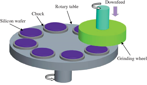
Wafer Backgrinding and Thickness Measurements in Semiconductor Manufacturing Wafer backgrinding, also known as wafer thinning or wafer lapping, is a critical step in semiconductor packaging. This process, which involves grinding the backside of a semiconductor wafer, reduces its thickness to enable the stacking of integrated circuits (ICs) and support high-density packaging. The thickness of the wafer plays a crucial role in determining the overall size of the package, an important factor as modern electronics such as smartphones, laptops, and other devices continue to get thinner and more compact. In applications like MEMS (Micro-Electro-Mechanical Systems), the backgrinding process also affects [...]
 Silicon Carbide vs. Silicon in EV Power Electronics Gallery
Silicon Carbide vs. Silicon in EV Power Electronics
Application Notes-MTI, Brand-MTI, Industry-Automotive, Industry-Battery, Industry-Compliance Testing, Industry-Consumer Products, Industry-Electronics, Industry-Government/Military, Industry-Manufacturing, Industry-R&D, News-MTI-Instrumentation, Products-MTI-Capacitance, Z-REPUB, z1
Silicon Carbide vs. Silicon in EV Power Electronics
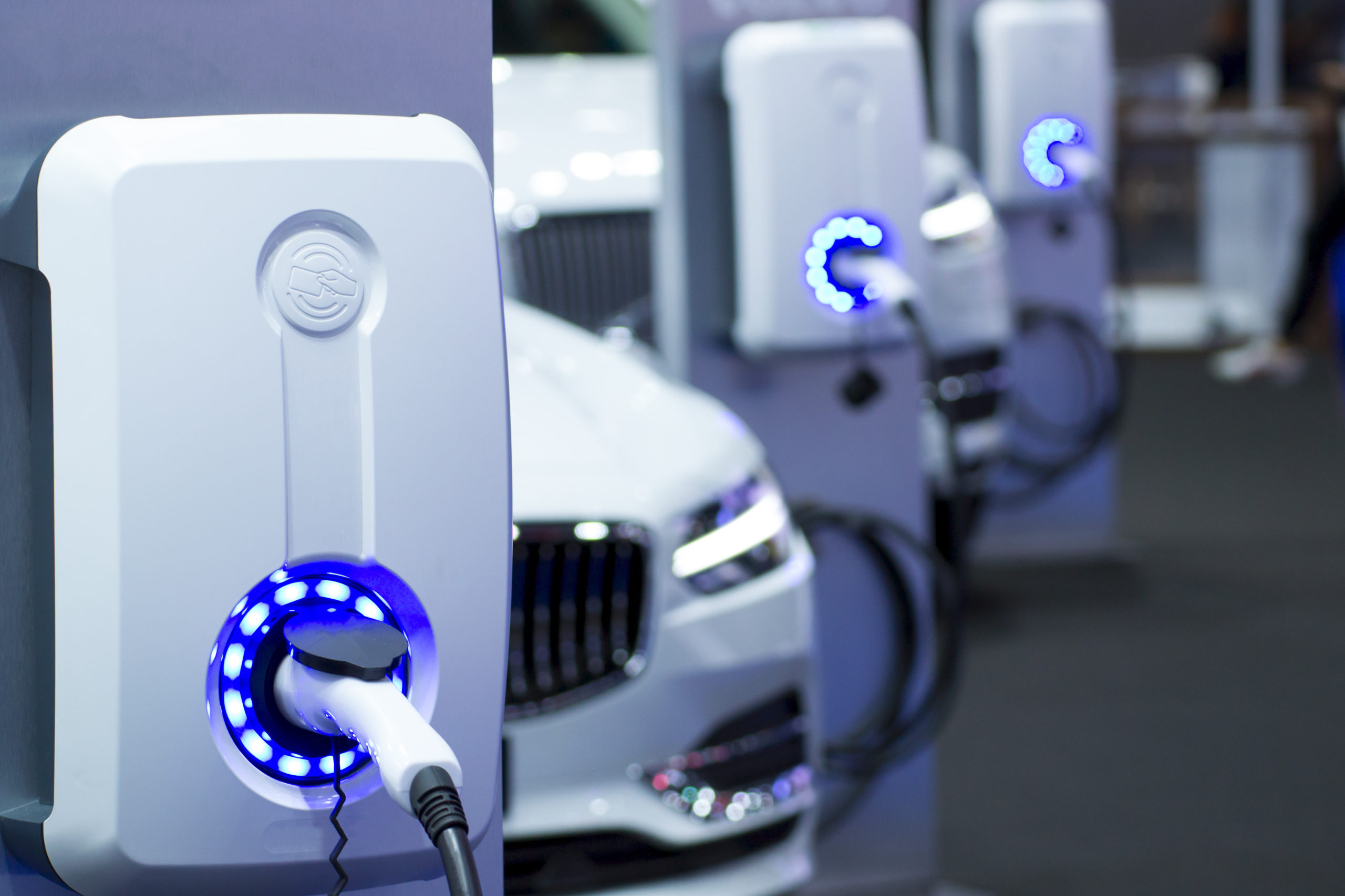
Compare silicon carbide vs. silicon for electric vehicle (EV) power electronics and learn about SiC wafer measurement. As demand for electric vehicles (EVs) continues to grow, manufacturers are comparing two semiconductor technologies, silicon carbide and silicon, for power electronics applications. Silicon carbide (SiC) provides the high temperature resistance, low power consumption, rigidity, and support for smaller, thinner designs that EV power electronics need. Examples of SiC’s current applications include on-board DC/DC converters, off-board DC fast chargers, on-board battery chargers, EV powertrains, and automotive lighting for LEDs. According to Automotive World, SiC technology could also drive future EV innovations [...]

Press Release: Vitrek Highlights Updated & Expanded Sections of their Website
Vitrek Highlights Updated & Expanded Sections of their Website The innovative high voltage testing and measurement company offers numerous resources for their customers on their website vitrek.com. […]
 MTI Instruments Fulfills Historic Order for the United States Air Force Gallery
MTI Instruments Fulfills Historic Order for the United States Air Force
Application Notes-Vitrek, Brand-MTI, Industry-Aerospace, Industry-Government/Military, New & Press Releases, News-MTI, News-MTI-PBS, Press Releases-Vitrek, z1

MTI Instruments Fulfills Historic Order for the United States Air Force
Lockport, IL, November 16, 2020 — MTI Instruments, Inc. (“MTI Instruments”), the operating subsidiary of Mechanical Technology, Incorporated (OTC Pink: MKTY), announces the completion of its historic order for the United States Air Force, a $3.3 million contract awarded publicly in May 2020 that includes 52 PBS-4100+ engine vibration measurement and balancing systems. This order was made pursuant to the multi-year contract entered into by MTI Instruments and the United States Air Force in July 2016 and marks the single largest order of PBS-4100+ Systems received by MTI Instruments to date. MTI fulfilled the order in its entirety with [...]
 White Paper: Electrical Safety & Compliance Testing for Appliance & Consumer Product Manufacturers Gallery
White Paper: Electrical Safety & Compliance Testing for Appliance & Consumer Product Manufacturers
Brand-Vitrek, Industry-Compliance Testing, Industry-Consumer Products, Industry-Electronics, Industry-Manufacturing, News-Vitrek, Products-Vitrek, Whitepapers-Vitrek, z1
White Paper: Electrical Safety & Compliance Testing for Appliance & Consumer Product Manufacturers
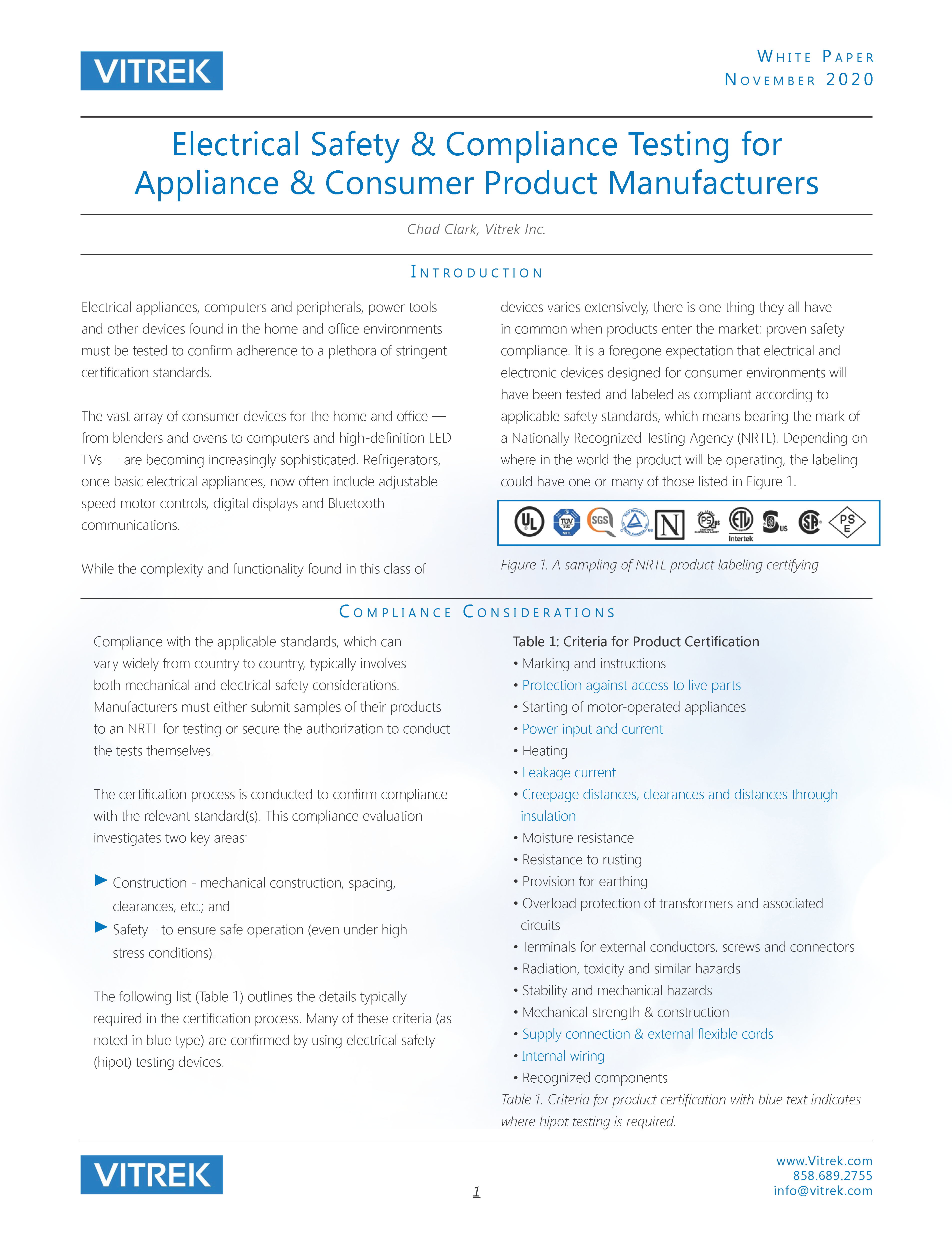
Introduction Electrical appliances, computers and peripherals, power tools and other devices found in the home and office environments must be tested to confirm adherence to a plethora of stringent certification standards. The vast array of consumer devices for the home and office — from blenders and ovens to computers and high-definition LED TVs — are becoming increasingly sophisticated. Refrigerators, once basic electrical appliances, now often include adjustable speed motor controls, digital displays and Bluetooth communications. While the complexity and functionality found in this class of devices varies extensively, there is one thing they all have in common when [...]
 Press Release: Vitrek Announces New SE Series High Voltage Safety Enclosures Gallery
Press Release: Vitrek Announces New SE Series High Voltage Safety Enclosures
Brand-Vitrek, Industry-Automotive, Industry-Cable Test, Industry-Compliance Testing, Industry-Consumer Products, Industry-Education, Industry-Electronics, Industry-Lighting, Industry-Manufacturing, New & Press Releases, News-Products, News-Vitrek, Press Releases-Vitrek, Products-Vitrek-Hipot, z1

Press Release: Vitrek Announces New SE Series High Voltage Safety Enclosures
Vitrek Announces the SE Series of High Voltage Safety Enclosures The SE Series offers the utmost in operator safety for high voltage testing with solid aluminum frame construction, a durable acrylic cover and a magnetic interlock safety switch. […]
 EV Batteries Need Thickness Gauging for Lower Costs and Higher Performance Gallery
EV Batteries Need Thickness Gauging for Lower Costs and Higher Performance
Application Notes-MTI, Brand-MTI, Industry-Automotive, Industry-Compliance Testing, Industry-Consumer Products, Industry-Electronics, Industry-Manufacturing, Industry: Transportation, News-MTI, Products-MTI, Products-MTI-Capacitance, Products-MTI-Laser/Fiber Optic, Z-REPUB, z1

EV Batteries Need Thickness Gauging for Lower Costs and Higher Performance
EV batteries need to cost less and last longer. Until the e-mobility industry solves these challenges, electric vehicle (EV) adoption won’t match the hype that’s driven by Tesla, the established automakers, and a host of startups who are attracting investors. According to Axios, the expense of owning an electric vehicle will exceed that of owning a conventional one until EV batteries cost less than $100/KWh to produce. Unfortunately, the EV industry isn’t expected to hit that target for another ten years. Yet, there is some encouraging news. Less expensive and better performing EV batteries are just a few years [...]
 Transducer Selection for High Resolution Applications Gallery
Transducer Selection for High Resolution Applications
Application Notes-MTI, Brand-MTI, News-MTI-Instrumentation, News-MTI-Metrology, News-Product Updates, News-Products, Products-MTI-Capacitance, Products-MTI-Laser/Fiber Optic, Products-MTI-Semiconductor/Metrology, Products-MTI-Signal Generators, Z-REPUB, z1
Transducer Selection for High Resolution Applications
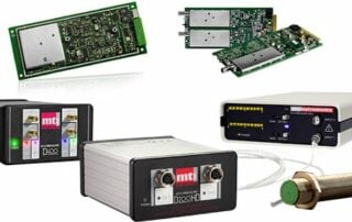
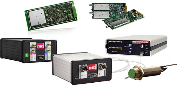
High resolution applications do not always require an interferometer. If you want to make accurate measurements in the micron to picometer range, then an MTI Digital Accumeasure D100 HD or D200 system may be what you need. Laser interferometers can sell for more than $15,000 and be difficult to setup. For example, you may have to buy additional optics to guarantee a good return signal since the laser beam must reflect off a mirror surface or precision retro reflector in order for the beam to re-enter the interferometer’s optics at less than a degree of reflection angle. The downsides [...]
High Resolution Semiconductor Wafer Measurements at Lower Costs
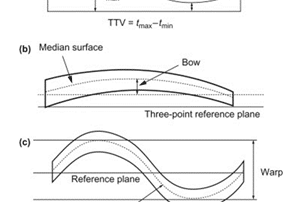
MTI's Proforma technology characterizes semiconductor wafers in terms of bow and warp, thickness, total thickness variation (TTV) and center thickness. Until recently, semiconductor wafer measurements at resolutions less than 100 µm were cost-prohibitive. Moreover, only expensive devices such as interferometers were capable of these measurements. Today, the semiconductor industry can use capacitance gauges instead of laser interferometers to achieve high resolution at fraction of the cost. Much like affordable CCD cameras transformed and expanded the market for video, cost-effective capacitance is disrupting the semiconductor wafer measurement market and creating new opportunities for quality testing and validation. The [...]
 Measure Wafer Bow, Warp and TTV with Capacitance Gallery
Measure Wafer Bow, Warp and TTV with Capacitance
Application Notes-MTI, Brand-MTI, Industry-Battery, Industry-Compliance Testing, Industry-Consumer Products, Industry-Electronics, Industry-Manufacturing, Industry-Semiconductor, Industry-Semiconductor-MTI, Industry-Sensors, Products-MTI-Capacitance, Z-REPUB, z1, ZOK

Measure Wafer Bow, Warp and TTV with Capacitance
The flatness of silicon wafers used to manufacture integrated circuits is controlled to tight tolerances to help ensure that the whole wafer is sufficiently flat for lithographic processing. To ensure your wafer manufacturing process is within tolerance, you need to measure the wafers being produced. Various measurement techniques exist to verify process tolerances and eliminate expensive scrap wafers. Non-contact capacitive sensing is a highly precise and cost-effective means to measure wafer flatness, bow, warp, and total thickness variation (TTV). MTI Instruments’ Proforma 300i and 300iSA systems use capacitance sensors to improve yields while reducing costs through better dimensional control of [...]