 White Paper: High Performance Test Equipment Assures LED Lighting Products Comply with Industry Standards Gallery
White Paper: High Performance Test Equipment Assures LED Lighting Products Comply with Industry Standards
Brand-Vitrek, Industry-Consumer Products, Industry-Lighting, News-Industry, News-Vitrek, Products-Vitrek, Whitepapers-Vitrek, z1
White Paper: High Performance Test Equipment Assures LED Lighting Products Comply with Industry Standards
Introduction Manufacturers and users of LED lighting applications need to be assured that their products will be qualified according to a multitude of reliability and efficiency standards. In addition to voluntary initiatives and programs like EnergyStar, mandatory standards and specifications for the lighting industry must be kept in mind during project development, including the latest IES LM-79-19 and the ANSI C82.16 documents. This article gives an overview of relevant lighting standards and specifications for LED lighting products. It also describes the features of Vitrek’s test equipment, including the PA900 power analyzer — featuring built-in lighting specifications — as [...]
 The Benefits of Manual, Semi-Automated, and Fully-Automated Systems for Semiconductor Wafer Inspection and Metrology Gallery
The Benefits of Manual, Semi-Automated, and Fully-Automated Systems for Semiconductor Wafer Inspection and Metrology
Application Notes-MTI, Brand-MTI, Industry-Consumer Products, Industry-Electronics, Industry-Manufacturing, Industry-Semiconductor, Industry-Semiconductor-MTI, News-MTI-Metrology, Products-MTI-Semiconductor/Metrology, z1
The Benefits of Manual, Semi-Automated, and Fully-Automated Systems for Semiconductor Wafer Inspection and Metrology
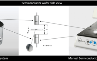
This is the third of three articles in Semiconductor Wafer Measurement for Increased Profitability. The first article in this series explains why disc geometry matters. The second article examines the cost of failing to inspect semiconductor wafers. Fully automated systems that can load, scan, and unload wafers are fast, convenient, and efficient at high volumes. They’re useful for checking every wafer in every batch, but these systems are expensive. Semi-automated and manual systems cost significantly less and are generally used for lower volumes; however, they’re also easy-to-use and can make fast, accurate measurements that support production flow. Semi-automated and [...]
 Why Disc Geometry Matters In Wafer Production Gallery
Why Disc Geometry Matters In Wafer Production
Application Notes-MTI, Brand-MTI, Industry-Consumer Products, Industry-Electronics, Industry-Manufacturing, Industry-Semiconductor, Industry-Semiconductor-MTI, News-MTI-Metrology, Products-MTI-Semiconductor/Metrology, z1
Why Disc Geometry Matters In Wafer Production
This is the first of three articles in Semiconductor Wafer Measurement for Increased Profitability. The second article examines the cost of failing to inspect semiconductor wafers. The third article describes the benefits of using semi-automated, fully-automated, and manual systems for wafer metrology and inspection. Semiconductor wafers are cut from cylindrical silicon crystals, or ingots. The flatness of these disc-shaped wafers is controlled to tight tolerances to ensure that the entire wafer surface is suitable for integrated circuit (IC) production. If disc geometry is out-of-spec after cutting, it may be possible to reprocess the wafer. Cutting is only the first [...]
 MTI Instruments Enters Advanced Qualification Stage for Electric Vehicle Battery Measurement Device with Several Major Automotive OEM Manufacturers Gallery
MTI Instruments Enters Advanced Qualification Stage for Electric Vehicle Battery Measurement Device with Several Major Automotive OEM Manufacturers
Brand-MTI, Industry-Automotive, Industry-Compliance Testing, Industry-Consumer Products, Industry-Manufacturing, New & Press Releases, News-MTI, Press Releases-Vitrek, z1
MTI Instruments Enters Advanced Qualification Stage for Electric Vehicle Battery Measurement Device with Several Major Automotive OEM Manufacturers
NEW YORK, December 16, 2021 – MTI Instruments division, a manufacturer of precision tools and testing equipment for electronics, aviation, automotive, power and other industries, today announced that it has entered into the advanced qualification stage for its electric vehicle (EV) battery measurement device with several major automotive OEM manufacturers. Moshe Binyamin, President and CEO of MTI Instruments commented, “We committed to shareholders that we would communicate with them as we began to get traction in the growing and large EV Battery manufacturing segment. I am pleased to report, we are gaining serious traction.” Binyamin further added, “In fact, [...]

How Capacitive Measurement Can Help Reduce Packaging Waste
Product packaging is often made of lightweight polymeric foams or plastic sheets and films. These materials are relatively inexpensive, but manufacturers still want to minimize waste and maximize yields. Across high volumes of low-cost materials, even a small per-unit savings can become significant, especially as the price of petroleum – a key ingredient in many polymers – continues to rise. For companies with environmental sustainability efforts, there are other important considerations as well. The excessive use of packaging materials can contribute to environmental pollution, especially with polymers that are slow to degrade. Yet, materials such as plastic sheets and [...]
 Contact vs. Non-Contact Measurement and Linear Displacement Sensors Gallery
Contact vs. Non-Contact Measurement and Linear Displacement Sensors
Application Notes-MTI, Brand-MTI, Industry-Compliance Testing, Industry-Consumer Products, Industry-Electronics, Industry-Manufacturing, Industry-Semiconductor, Industry-Semiconductor-MTI, Industry-Sensors, Products-MTI-Capacitance, Z-REPUB, z1, ZOK
Contact vs. Non-Contact Measurement and Linear Displacement Sensors
Contact vs. Non-Contact Measurements Choosing between a contact measurement system and a non-contact measurement system requires careful evaluation of your application’s performance needs, material properties, environmental conditions, and measurement goals. Each system type offers unique advantages- and understanding these distinctions can help you make a more informed decision. Let's explores how contact and non-contact measurement techniques work, their strengths and limitations, and where they’re best applied. What Are Contact Measurement Systems? Contact measurement systems involve tools and sensors that physically touch the object to determine various physical characteristics. These systems are widely used in dimensional metrology, offering high precision, [...]
Foam Density Measurement: Capacitance Sensors vs. Nuclear Gauges
This application note from MTI Instruments compares two technologies for measuring foam density: capacitance sensors and nuclear gauges. It examines the basic operating principles of each technology and explains why capacitance measurement is recommended for in-line measurement during foam manufacturing. Capacitance Sensors Capacitive probes are non-contact devices that use electric fields to measure foam density. In combination with a thickness value, a density measurement may be calculated. These probes consist of a capacitance sensor inside of a protective housing and are part of a larger measurement system that includes amplifiers, cables, and software. With parallel plate capacitance, the capacitance probe [...]
 Using Capacitance Sensors for Non-Conductive Material Measurement Gallery
Using Capacitance Sensors for Non-Conductive Material Measurement
Application Notes-MTI, Brand-MTI, Industry-Compliance Testing, Industry-Consumer Products, Industry-Electronics, Industry-Manufacturing, Industry-Sensors, News-MTI, News-MTI-Instrumentation, Products-MTI-Capacitance, Z-REPUB, z1
Using Capacitance Sensors for Non-Conductive Material Measurement
Non-Conductive Material Measurement with Capacitance Sensors Capacitance sensors are non-contact devices that can be used to obtain position, thickness, and dynamic measurements with a high degree of precision, accuracy, and resolution. Capacitive measurement is used with electrically-conductive materials such as metals but can also be used to measure non-conductive materials such as glass, sapphire, and many plastics. Even if a non-conductive material is relatively inexpensive (such as closed cell foam), manufacturers want to avoid errors that can result in significant waste across high volumes. Importantly, capacitance measurement is also used with semi-insulating materials such as gallium arsenide (GaAs) and [...]
 Why Demand for SiC Wafers is Soaring and Durable Gallery
Why Demand for SiC Wafers is Soaring and Durable
Brand-MTI, Industry-Consumer Products, Industry-Electronics, Industry-Manufacturing, Industry-Semiconductor, Industry-Semiconductor-MTI, MTI Blog, News-MTI, News-MTI-Metrology, Products-MTI-Semiconductor/Metrology, Z-REPUB, z1
Why Demand for SiC Wafers is Soaring and Durable
Silicon carbide (SiC) wafers are in high demand, particularly in high-temperature applications. Silicon carbide (SiC), a semiconductor material made of both silicon and carbon, can withstand extreme temperatures of up to 2700°C. Often referred to as carborundum, SiC’s unique properties also make it a key material in non-electronic applications such as bulletproof vests, extrusion dies, sandpaper, and high-performance disc brakes. In the electronics industry, SiC wafers are crucial for devices operating under high temperatures, high voltages, or both. For example, they are used in electric vehicle (EV) power electronics, 5G communication systems, and LED technology, making SiC a material [...]
Wafer Stress Analysis Using the 300iSA
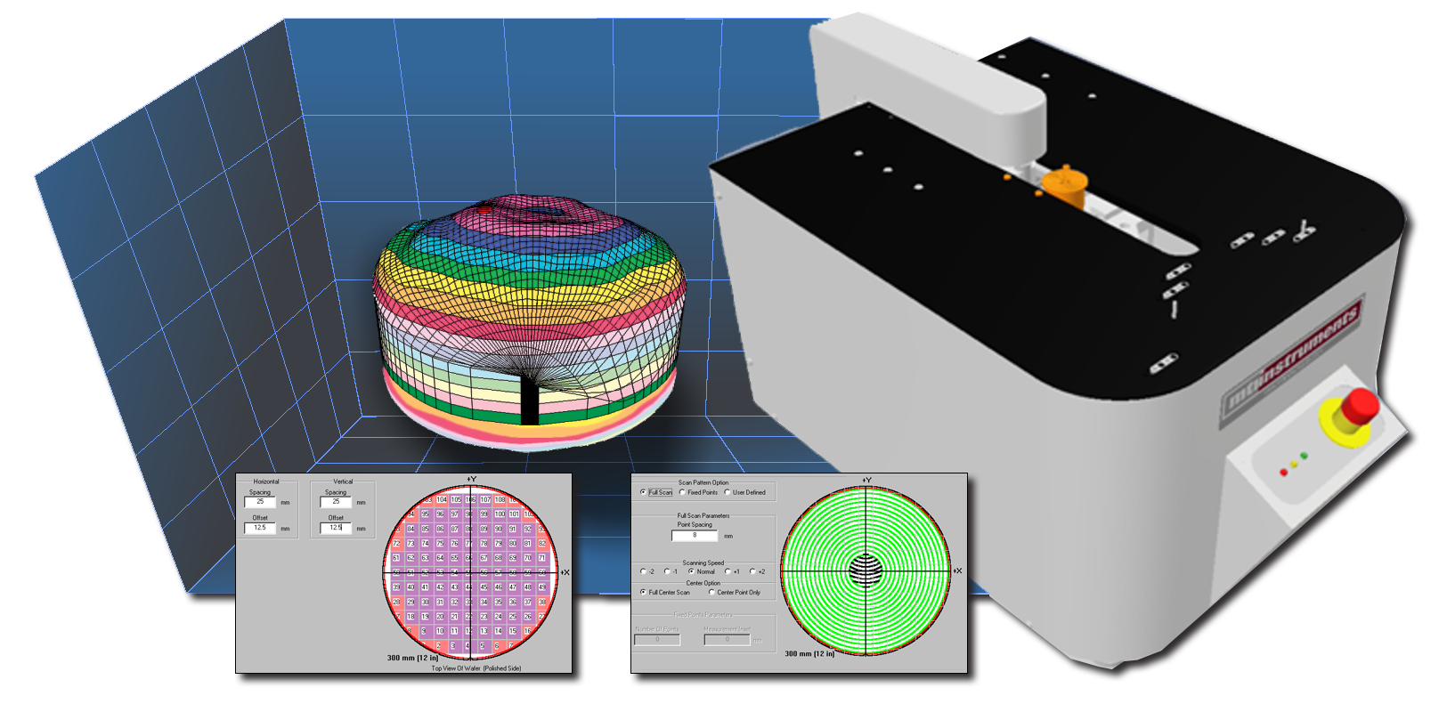
Wafer Stress Analysis Using MTI Instruments Proforma 300iSA Wafer processing involves several stages that can lead to mechanical changes in the wafer structure. These changes, or stresses, may result in deformities, making the wafer either unusable or only marginally usable. To evaluate these stresses and determine the wafer's quality, wafer stress measurement is essential. The Proforma 300iSA wafer characterization tool offers a powerful solution for wafer stress analysis. It allows for the analysis of a wafer both before and after processing. By comparing these two states, the Proforma 300iSA effectively evaluates the wafer's stress levels and mechanical alterations, providing [...]