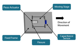
Capacitance Probes vs. Strain Gauges in Piezo Flexure Stages
Capacitance probes with pico-positioning sensors can be embedded in piezo flexure stages. With minor mounting modifications, these non-contact probes provide significantly greater accuracy than strain gauges. Piezo flexure stages are positioning devices with a high degree of resolution. These motion stages contain a piezoelectric actuator that converts an electrical signal into displacement based on the reverse piezoelectric effect, which is the ability of a piezo electric material to elongate when a voltage is applied. When a voltage (e.g., 0-150 VDC) is applied to the actuator, the stage moves in proportion to the applied voltage. Yet, the exact position remains [...]
 CMP and Capacitance-Based Semiconductor Wafer Measurement Gallery
CMP and Capacitance-Based Semiconductor Wafer Measurement
Application Notes-MTI, Brand-MTI, Industry-Compliance Testing, Industry-Consumer Products, Industry-Electronics, Industry-Manufacturing, Industry-Semiconductor, Industry-Semiconductor-MTI, Industry-Sensors, Products-MTI-Capacitance, Products-MTI-Semiconductor/Metrology, z1
CMP and Capacitance-Based Semiconductor Wafer Measurement
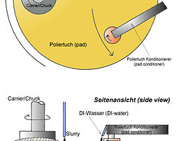
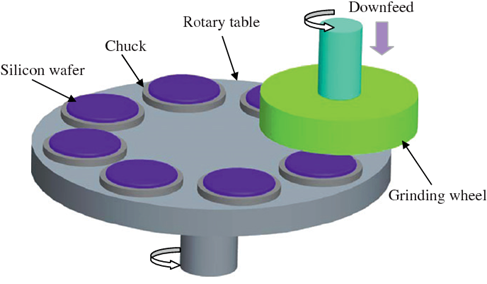
Chemical mechanical polishing (CMP) uses chemical oxidation and mechanical abrasion to selectively remove material from semiconductor wafers in order to achieve very high levels of planarity. The planarity, or flatness, of these wafers is important for optical lithography, a microfabrication technique that produces integrated circuits (ICs) by transferring a geometric pattern from a photomask to a light-sensitive chemical photoresist. Also known as photolithography or UV lithography, optical lithography can produce a geometric pattern on a thin film or directly onto the substrate. Semiconductor Wafer Measurements: Flatness and Shape During optical lithography, variations in wafer flatness must be smaller than [...]
 MEMS and Capacitance-Based Semiconductor Wafer Measurement Gallery
MEMS and Capacitance-Based Semiconductor Wafer Measurement
Application Notes-MTI, Brand-MTI, Industry-Compliance Testing, Industry-Consumer Products, Industry-Electronics, Industry-Manufacturing, Industry-Semiconductor, Industry-Semiconductor-MTI, Industry-Sensors, Products-MTI-Capacitance, Products-MTI-Semiconductor/Metrology, Z-REPUB, z1
MEMS and Capacitance-Based Semiconductor Wafer Measurement
MEMS Technology and Capacitance-Based Wafer Measurement Micro-electrical-mechanical systems (MEMS) are tiny devices that house electrical and mechanical components on a single silicon chip or integrated circuit (IC). They integrate mechanical structures with electronics that are normally fabricated with complementary metal-oxide-semiconductor (CMOS) technologies. In addition to miniaturization, the benefits of MEMS include expanded functionalities at lower cost and with improved performance and reliability. With MEMS devices, critical physical dimensions range from smaller than one micron (µ) to larger than several millimeters (mm). In complex systems, multiple moving elements may be controlled by integrated electronics. Examples of the mechanical components in [...]
Measuring the Step Height Thickness of Non- Woven Conductive Films
Establishing and maintaining product quality throughout the production process is a common challenge of all manufacturers. How does an organization ensure the optimal output from their production lines, especially in real time? Key to this is strong non-destructive measurement practices that can take place at various points along the production process. The case study below is an example of how this was done at Saint-Gobain to measure the thickness and density of foam materials. They engaged with MTI's team of experts as their current direction was proving cost-prohibitive. Saint-Gobain's R&D organization, led by Dr. Mickael Boinet, found a solution [...]
Webinar Recap: Electrical Safety Testing for the Appliance & Consumer Product Industries
Vitrek is proud to hold educational webinars for our customers in various industries with information and products that are relevant to their applications. One such industry that relies on some of the technology that we offer is the appliance and consumer products industry, which requires extensive electrical safety testing in order to bring their products to market. All products that will be sold to consumers need to be tested by a Nationally Recognized Testing Laboratory (NRTL) in order to earn the proper safety certification. […]
 Wafer Backgrinding and Semiconductor Thickness Measurements Gallery
Wafer Backgrinding and Semiconductor Thickness Measurements
Application Notes-MTI, Brand-MTI, Industry-Compliance Testing, Industry-Consumer Products, Industry-Electronics, Industry-Manufacturing, Industry-Semiconductor, Industry-Semiconductor-MTI, News-MTI-Instrumentation, News-MTI-Metrology, Products-MTI-Capacitance, Products-MTI-Semiconductor/Metrology, Z-REPUB, z1

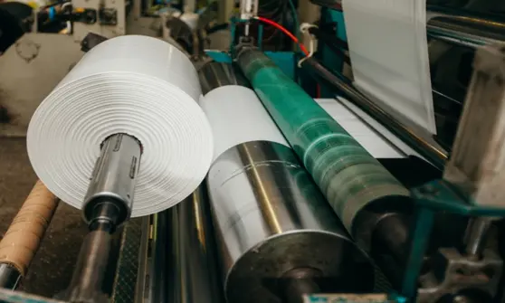
Wafer Backgrinding and Semiconductor Thickness Measurements
Wafer Backgrinding and Thickness Measurements in Semiconductor Manufacturing Wafer backgrinding, also known as wafer thinning or wafer lapping, is a critical step in semiconductor packaging. This process, which involves grinding the backside of a semiconductor wafer, reduces its thickness to enable the stacking of integrated circuits (ICs) and support high-density packaging. The thickness of the wafer plays a crucial role in determining the overall size of the package, an important factor as modern electronics such as smartphones, laptops, and other devices continue to get thinner and more compact. In applications like MEMS (Micro-Electro-Mechanical Systems), the backgrinding process also affects [...]
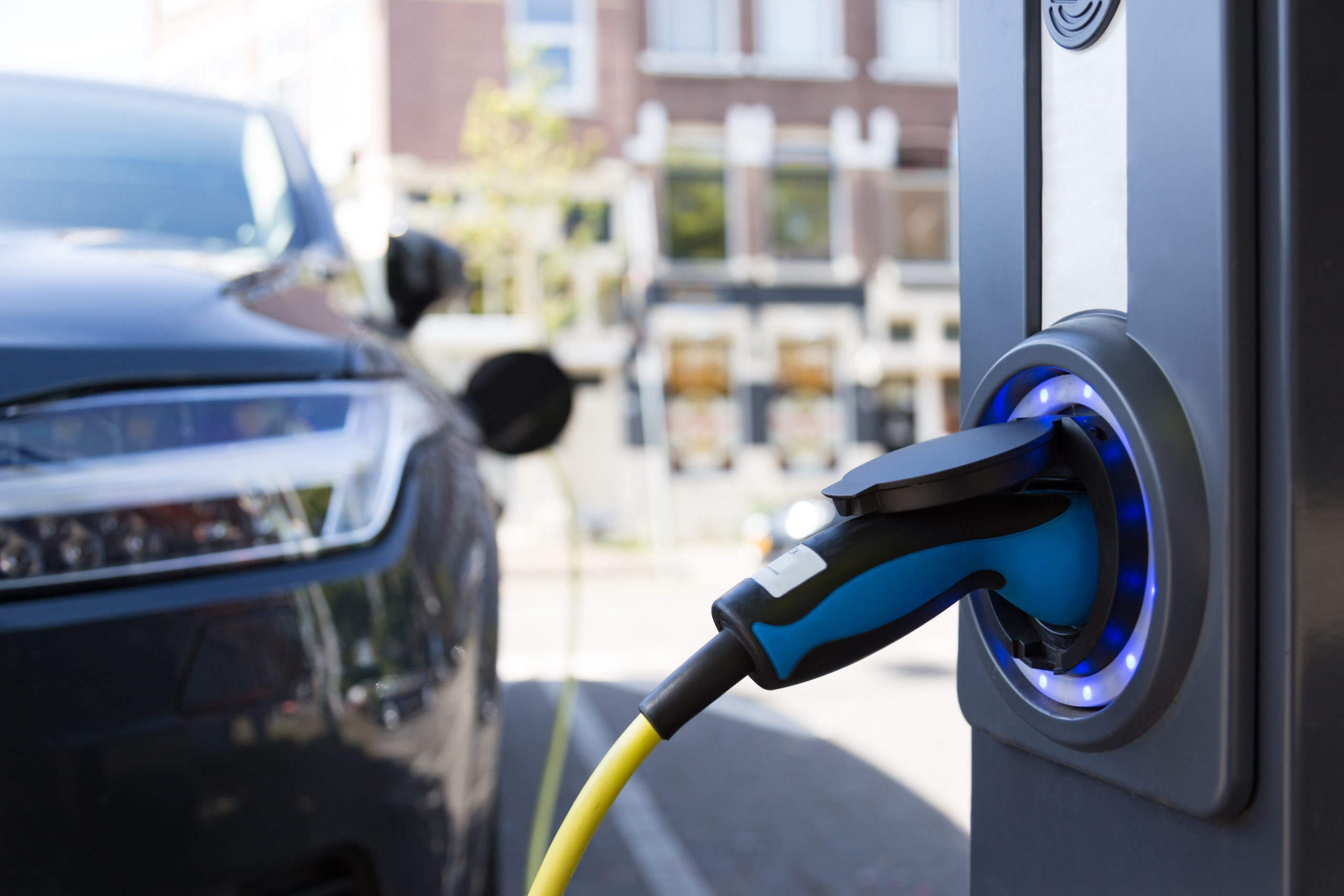
 Silicon Carbide vs. Silicon in EV Power Electronics Gallery
Silicon Carbide vs. Silicon in EV Power Electronics
Application Notes-MTI, Brand-MTI, Industry-Automotive, Industry-Battery, Industry-Compliance Testing, Industry-Consumer Products, Industry-Electronics, Industry-Government/Military, Industry-Manufacturing, Industry-R&D, News-MTI-Instrumentation, Products-MTI-Capacitance, Z-REPUB, z1
Silicon Carbide vs. Silicon in EV Power Electronics
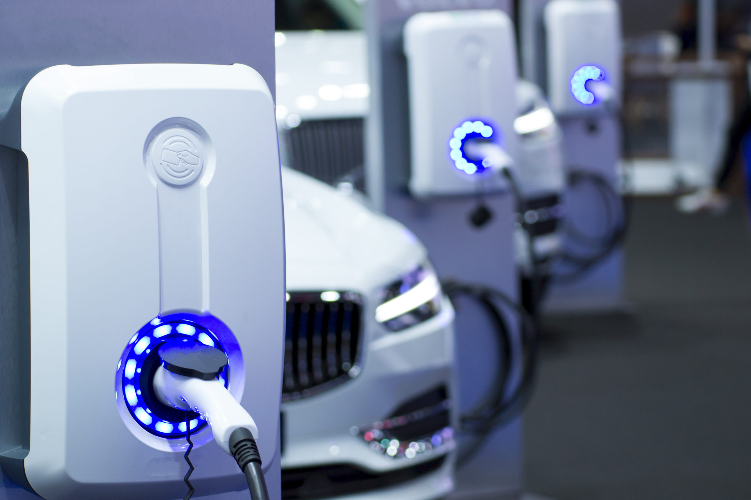
Compare silicon carbide vs. silicon for electric vehicle (EV) power electronics and learn about SiC wafer measurement. As demand for electric vehicles (EVs) continues to grow, manufacturers are comparing two semiconductor technologies, silicon carbide and silicon, for power electronics applications. Silicon carbide (SiC) provides the high temperature resistance, low power consumption, rigidity, and support for smaller, thinner designs that EV power electronics need. Examples of SiC’s current applications include on-board DC/DC converters, off-board DC fast chargers, on-board battery chargers, EV powertrains, and automotive lighting for LEDs. According to Automotive World, SiC technology could also drive future EV innovations [...]
 White Paper: Electrical Safety & Compliance Testing for Appliance & Consumer Product Manufacturers Gallery
White Paper: Electrical Safety & Compliance Testing for Appliance & Consumer Product Manufacturers
Brand-Vitrek, Industry-Compliance Testing, Industry-Consumer Products, Industry-Electronics, Industry-Manufacturing, News-Vitrek, Products-Vitrek, Whitepapers-Vitrek, z1
White Paper: Electrical Safety & Compliance Testing for Appliance & Consumer Product Manufacturers
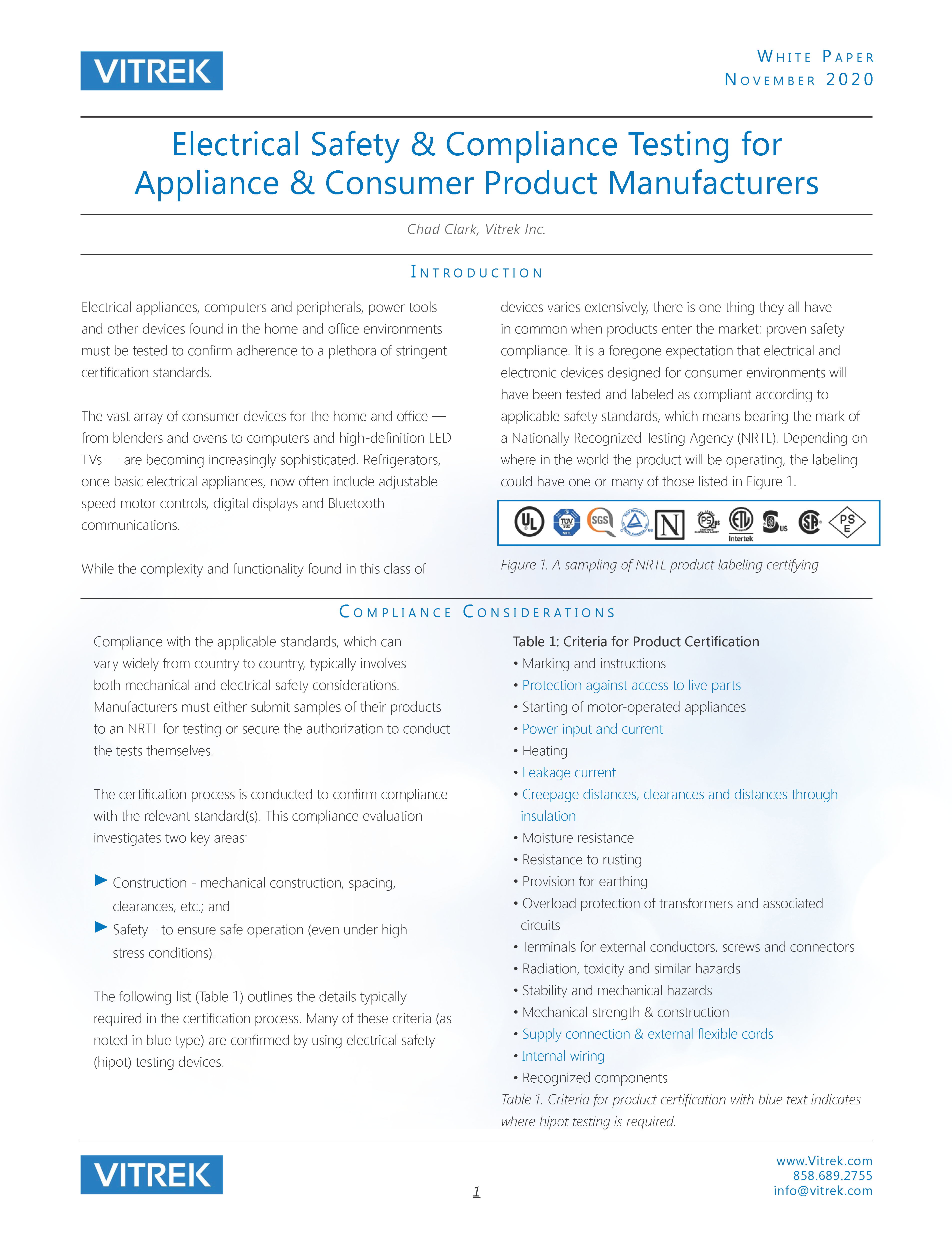
Introduction Electrical appliances, computers and peripherals, power tools and other devices found in the home and office environments must be tested to confirm adherence to a plethora of stringent certification standards. The vast array of consumer devices for the home and office — from blenders and ovens to computers and high-definition LED TVs — are becoming increasingly sophisticated. Refrigerators, once basic electrical appliances, now often include adjustable speed motor controls, digital displays and Bluetooth communications. While the complexity and functionality found in this class of devices varies extensively, there is one thing they all have in common when [...]
 Press Release: Vitrek Announces New SE Series High Voltage Safety Enclosures Gallery
Press Release: Vitrek Announces New SE Series High Voltage Safety Enclosures
Brand-Vitrek, Industry-Automotive, Industry-Cable Test, Industry-Compliance Testing, Industry-Consumer Products, Industry-Education, Industry-Electronics, Industry-Lighting, Industry-Manufacturing, New & Press Releases, News-Products, News-Vitrek, Press Releases-Vitrek, Products-Vitrek-Hipot, z1
Press Release: Vitrek Announces New SE Series High Voltage Safety Enclosures
Vitrek Announces the SE Series of High Voltage Safety Enclosures The SE Series offers the utmost in operator safety for high voltage testing with solid aluminum frame construction, a durable acrylic cover and a magnetic interlock safety switch. […]
 EV Batteries Need Thickness Gauging for Lower Costs and Higher Performance Gallery
EV Batteries Need Thickness Gauging for Lower Costs and Higher Performance
Application Notes-MTI, Brand-MTI, Industry-Automotive, Industry-Compliance Testing, Industry-Consumer Products, Industry-Electronics, Industry-Manufacturing, Industry: Transportation, News-MTI, Products-MTI, Products-MTI-Capacitance, Products-MTI-Laser/Fiber Optic, Z-REPUB, z1
EV Batteries Need Thickness Gauging for Lower Costs and Higher Performance
EV batteries need to cost less and last longer. Until the e-mobility industry solves these challenges, electric vehicle (EV) adoption won’t match the hype that’s driven by Tesla, the established automakers, and a host of startups who are attracting investors. According to Axios, the expense of owning an electric vehicle will exceed that of owning a conventional one until EV batteries cost less than $100/KWh to produce. Unfortunately, the EV industry isn’t expected to hit that target for another ten years. Yet, there is some encouraging news. Less expensive and better performing EV batteries are just a few years [...]