

Capacitive Displacement Sensors: Working Principle & Precision Measurement Applications
Capacitive Displacement Sensors: Working Principle & Precision Measurement Applications Capacitive displacement sensors are precision non-contact measurement devices that utilize capacitance changes to determine position, distance, and thickness with exceptional accuracy. These capacitive distance sensors offer superior performance in applications requiring high-resolution measurements, making them essential tools across manufacturing, automation, and research industries. How Capacitive Displacement Sensors Work Capacitive Sensor Working Principle Capacitive displacement sensors operate on the fundamental principle of measuring capacitance variations between two conductive surfaces. The sensor probe acts as one plate of a parallel plate capacitor, while the [...]
 MTI Instrument’s PBS ROI Calculator: See How Much Money You Can Save Gallery
MTI Instrument’s PBS ROI Calculator: See How Much Money You Can Save
Application Notes-MTI, Brand-MTI, Industry-Aerospace, Industry-Compliance Testing, Industry-Government/Military, Industry-Manufacturing, Industry: Transportation, New & Press Releases, News-MTI, News-MTI-PBS, News-Products, Press Releases-Vitrek, Products-MTI, Products-MTI-Engine Balancing, Z-REPUB, z1
MTI Instrument’s PBS ROI Calculator: See How Much Money You Can Save
Ensuring the proper operation of your aircraft engine is essential to complying with manufacturers guidelines for the safety and longevity of the aircraft. Ensuring engines are not operating outside acceptible vibration limits and operating optimally isn't just smart, it is vital to your business. Excessive engine vibration can lead to cracked turbine, fan and compressor components potentially leading to catastrophic failure. The costs of catastrophic engine failure due to an unbalanced engine can measure in the millions of dollars. As airlines push to get more and more life out of their aging fleets, the need to properly maintain the [...]
 Multinational Manufacturer Saint-Gobain Selects MTI Instruments’ Digital Capacitance Measurement Technology to Streamline R&D Gallery
Multinational Manufacturer Saint-Gobain Selects MTI Instruments’ Digital Capacitance Measurement Technology to Streamline R&D
Brand-MTI, Industry-Manufacturing, Industry-R&D, New & Press Releases, News-MTI-Instrumentation, Press Releases-Vitrek, Products-MTI-Capacitance, Z-REPUB, z1
Multinational Manufacturer Saint-Gobain Selects MTI Instruments’ Digital Capacitance Measurement Technology to Streamline R&D
Multinational Manufacturer Saint-Gobain Selects MTI Instruments’ Digital Capacitance Measurement Technology to Streamline R&D Lockport, IL, April 21, 2021 /PRNewswire/ — MTI Instruments, Inc. (“MTI Instruments”), a wholly-owned subsidiary of Mechanical Technology, Incorporated (NASDAQ: MKTY), announced today that Compagnie de Saint-Gobain (“Saint-Gobain”) has selected MTI Instruments’ non-destructive measurement technology to help streamline the Saint-Gobain’s manufacturing research and development. Saint-Gobain, a French multinational corporation that designs, manufactures, and distributes various high-performance materials, chose MTI Instruments as a partner after identifying that the process for producing accurate and repeatable measurement solutions was time-consuming and cost-prohibitive. Saint-Gobain estimated that just 30% of their process [...]
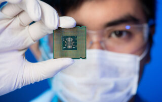 MEMS and Capacitance-Based Semiconductor Wafer Measurement Gallery
MEMS and Capacitance-Based Semiconductor Wafer Measurement
Application Notes-MTI, Brand-MTI, Industry-Compliance Testing, Industry-Consumer Products, Industry-Electronics, Industry-Manufacturing, Industry-Semiconductor, Industry-Semiconductor-MTI, Industry-Sensors, Products-MTI-Capacitance, Products-MTI-Semiconductor/Metrology, Z-REPUB, z1
MEMS and Capacitance-Based Semiconductor Wafer Measurement
MEMS Technology and Capacitance-Based Wafer Measurement Micro-electrical-mechanical systems (MEMS) are tiny devices that house electrical and mechanical components on a single silicon chip or integrated circuit (IC). They integrate mechanical structures with electronics that are normally fabricated with complementary metal-oxide-semiconductor (CMOS) technologies. In addition to miniaturization, the benefits of MEMS include expanded functionalities at lower cost and with improved performance and reliability. With MEMS devices, critical physical dimensions range from smaller than one micron (µ) to larger than several millimeters (mm). In complex systems, multiple moving elements may be controlled by integrated electronics. Examples of the mechanical components in [...]

PAxx Power Analyzers using External Current Sensors: Application Notes
Current Sensors use two main techniques. A current transformer divides current. So for instance a 100:1 current transformer would see an input of 10A and output 100mA. Note that this technique is only useful for AC current. When using a current transformer you can directly input the current into one of our internal shunts as long as you stay within the current limitations of the input. Notice that current transformers are inductive so they act as a low pass filter. If you use a current transformer it is important to select a transformer that will work accurately at your frequency [...]
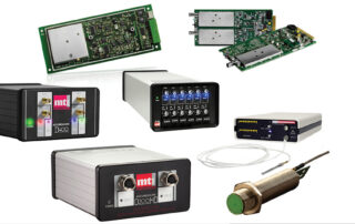 MTI Instruments’ Accumeasure HD System Proven to Be Highest Resolution Capacitance System in the World Gallery
MTI Instruments’ Accumeasure HD System Proven to Be Highest Resolution Capacitance System in the World
Blog, Brand-MTI, Industry-Sensors, New & Press Releases, News-MTI, Press Releases-Vitrek, Products-MTI-Capacitance, Z-REPUB, z1
MTI Instruments’ Accumeasure HD System Proven to Be Highest Resolution Capacitance System in the World
Lockport, IL, April 9, 2021 /PRNewswire/ — MTI Instruments, Inc. (“MTI Instruments”), a wholly-owned subsidiary of Mechanical Technology, Incorporated, (NASDAQ: MKTY), announced today that its Accumeasure HD system technology has been proven to measure distances as small as 69 picometers, setting a new bar for capacitance systems. The results were recently published in a white paper by Kevin Harding of Optical Metrology Solutions. Harding’s white paper can be accessed on MTI Instruments’ website. Harding’s independent study confirmed the findings of an internal experiment by MTI Instruments that concluded the Accumeasure HD system can provide picometer-level accuracy when used with [...]
Webinar Recap: Vitrek Electrical Safety Testing for the Automotive Industry
Vitrek is a leading provider of testing solutions for electrical safety across multiple industries. Headquartered in San Diego, CA, and in business for over three decades, Vitrek has established itself as one of the premier electrical safety testing companies on the market. They serve over 30 different countries and provide electrical safety testing equipment that can be utilized in countless applications. […]
 Press Release: Vitrek Expands into the DAQ Market by Acquiring Dynamic Signals Gallery
Press Release: Vitrek Expands into the DAQ Market by Acquiring Dynamic Signals
Brand-GaGe, Brand-Vitrek, Brands-All, New & Press Releases, News-All Brands, News-GaGe, News-Industry, News-Vitrek, Press Releases-Vitrek, z1
Press Release: Vitrek Expands into the DAQ Market by Acquiring Dynamic Signals
Vitrek Expands into the DAQ Market by Acquiring DynamicSignals Expands Vitrek product portfolio to include high-performance signal capture and processing solutions; Integration of global engineering, sales and production strengthens reach in semiconductor, pharmaceutical and mil/aero industries. […]
Applications by Industry
Vitrek is a world leader in providing safety and electrical test equipment, solar & metrology systems, vibration/engine balancing systems, high-speed data acquisition and real-time signal recording solutions to a range of industries including electronic, appliance and automotive manufacturers, calibration & test labs, R & D departments, medical, aerospace, military and lighting. Offering both the best equipment and top-notch support, choose Vitrek for your next test, measurement and high-speed data acquisition equipment needs. Choose from industries below to see how Vitrek products can help improve quality and efficiency in your business. [...]



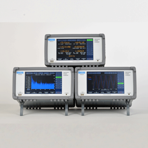
Measuring the Step Height Thickness of Non- Woven Conductive Films
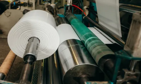
Establishing and maintaining product quality throughout the production process is a common challenge of all manufacturers. How does an organization ensure the optimal output from their production lines, especially in real time? Key to this is strong non-destructive measurement practices that can take place at various points along the production process. The case study below is an example of how this was done at Saint-Gobain to measure the thickness and density of foam materials. They engaged with MTI's team of experts as their current direction was proving cost-prohibitive. Saint-Gobain's R&D organization, led by Dr. Mickael Boinet, found a solution [...]