Wafer Stress Analysis Using the 300iSA
Wafer Stress Analysis Using MTI Instruments Proforma 300iSA Wafer processing involves several stages that can lead to mechanical changes in the wafer structure. These changes, or stresses, may result in deformities, making the wafer either unusable or only marginally usable. To evaluate these stresses and determine the wafer's quality, wafer stress measurement is essential. The Proforma 300iSA wafer characterization tool offers a powerful solution for wafer stress analysis. It allows for the analysis of a wafer both before and after processing. By comparing these two states, the Proforma 300iSA effectively evaluates the wafer's stress levels and mechanical alterations, providing [...]
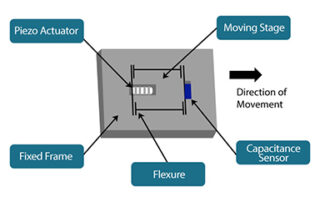
Capacitance Probes vs. Strain Gauges in Piezo Flexure Stages
Capacitance probes with pico-positioning sensors can be embedded in piezo flexure stages. With minor mounting modifications, these non-contact probes provide significantly greater accuracy than strain gauges. Piezo flexure stages are positioning devices with a high degree of resolution. These motion stages contain a piezoelectric actuator that converts an electrical signal into displacement based on the reverse piezoelectric effect, which is the ability of a piezo electric material to elongate when a voltage is applied. When a voltage (e.g., 0-150 VDC) is applied to the actuator, the stage moves in proportion to the applied voltage. Yet, the exact position remains [...]
 CMP and Capacitance-Based Semiconductor Wafer Measurement Gallery
CMP and Capacitance-Based Semiconductor Wafer Measurement
Application Notes-MTI, Brand-MTI, Industry-Compliance Testing, Industry-Consumer Products, Industry-Electronics, Industry-Manufacturing, Industry-Semiconductor, Industry-Semiconductor-MTI, Industry-Sensors, Products-MTI-Capacitance, Products-MTI-Semiconductor/Metrology, z1
CMP and Capacitance-Based Semiconductor Wafer Measurement
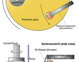
Chemical mechanical polishing (CMP) uses chemical oxidation and mechanical abrasion to selectively remove material from semiconductor wafers in order to achieve very high levels of planarity. The planarity, or flatness, of these wafers is important for optical lithography, a microfabrication technique that produces integrated circuits (ICs) by transferring a geometric pattern from a photomask to a light-sensitive chemical photoresist. Also known as photolithography or UV lithography, optical lithography can produce a geometric pattern on a thin film or directly onto the substrate. Semiconductor Wafer Measurements: Flatness and Shape During optical lithography, variations in wafer flatness must be smaller than [...]
 MTI Instrument’s PBS ROI Calculator: See How Much Money You Can Save Gallery
MTI Instrument’s PBS ROI Calculator: See How Much Money You Can Save
Application Notes-MTI, Brand-MTI, Industry-Aerospace, Industry-Compliance Testing, Industry-Government/Military, Industry-Manufacturing, Industry: Transportation, New & Press Releases, News-MTI, News-MTI-PBS, News-Products, Press Releases-Vitrek, Products-MTI, Products-MTI-Engine Balancing, Z-REPUB, z1

MTI Instrument’s PBS ROI Calculator: See How Much Money You Can Save
Ensuring the proper operation of your aircraft engine is essential to complying with manufacturers guidelines for the safety and longevity of the aircraft. Ensuring engines are not operating outside acceptible vibration limits and operating optimally isn't just smart, it is vital to your business. Excessive engine vibration can lead to cracked turbine, fan and compressor components potentially leading to catastrophic failure. The costs of catastrophic engine failure due to an unbalanced engine can measure in the millions of dollars. As airlines push to get more and more life out of their aging fleets, the need to properly maintain the [...]
 MEMS and Capacitance-Based Semiconductor Wafer Measurement Gallery
MEMS and Capacitance-Based Semiconductor Wafer Measurement
Application Notes-MTI, Brand-MTI, Industry-Compliance Testing, Industry-Consumer Products, Industry-Electronics, Industry-Manufacturing, Industry-Semiconductor, Industry-Semiconductor-MTI, Industry-Sensors, Products-MTI-Capacitance, Products-MTI-Semiconductor/Metrology, Z-REPUB, z1
MEMS and Capacitance-Based Semiconductor Wafer Measurement
MEMS Technology and Capacitance-Based Wafer Measurement Micro-electrical-mechanical systems (MEMS) are tiny devices that house electrical and mechanical components on a single silicon chip or integrated circuit (IC). They integrate mechanical structures with electronics that are normally fabricated with complementary metal-oxide-semiconductor (CMOS) technologies. In addition to miniaturization, the benefits of MEMS include expanded functionalities at lower cost and with improved performance and reliability. With MEMS devices, critical physical dimensions range from smaller than one micron (µ) to larger than several millimeters (mm). In complex systems, multiple moving elements may be controlled by integrated electronics. Examples of the mechanical components in [...]

Measuring the Step Height Thickness of Non- Woven Conductive Films
Establishing and maintaining product quality throughout the production process is a common challenge of all manufacturers. How does an organization ensure the optimal output from their production lines, especially in real time? Key to this is strong non-destructive measurement practices that can take place at various points along the production process. The case study below is an example of how this was done at Saint-Gobain to measure the thickness and density of foam materials. They engaged with MTI's team of experts as their current direction was proving cost-prohibitive. Saint-Gobain's R&D organization, led by Dr. Mickael Boinet, found a solution [...]
 Wafer Backgrinding and Semiconductor Thickness Measurements Gallery
Wafer Backgrinding and Semiconductor Thickness Measurements
Application Notes-MTI, Brand-MTI, Industry-Compliance Testing, Industry-Consumer Products, Industry-Electronics, Industry-Manufacturing, Industry-Semiconductor, Industry-Semiconductor-MTI, News-MTI-Instrumentation, News-MTI-Metrology, Products-MTI-Capacitance, Products-MTI-Semiconductor/Metrology, Z-REPUB, z1

Wafer Backgrinding and Semiconductor Thickness Measurements
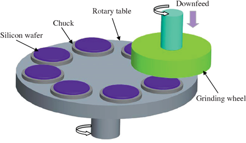
Wafer Backgrinding and Thickness Measurements in Semiconductor Manufacturing Wafer backgrinding, also known as wafer thinning or wafer lapping, is a critical step in semiconductor packaging. This process, which involves grinding the backside of a semiconductor wafer, reduces its thickness to enable the stacking of integrated circuits (ICs) and support high-density packaging. The thickness of the wafer plays a crucial role in determining the overall size of the package, an important factor as modern electronics such as smartphones, laptops, and other devices continue to get thinner and more compact. In applications like MEMS (Micro-Electro-Mechanical Systems), the backgrinding process also affects [...]
 Silicon Carbide vs. Silicon in EV Power Electronics Gallery
Silicon Carbide vs. Silicon in EV Power Electronics
Application Notes-MTI, Brand-MTI, Industry-Automotive, Industry-Battery, Industry-Compliance Testing, Industry-Consumer Products, Industry-Electronics, Industry-Government/Military, Industry-Manufacturing, Industry-R&D, News-MTI-Instrumentation, Products-MTI-Capacitance, Z-REPUB, z1
Silicon Carbide vs. Silicon in EV Power Electronics
Compare silicon carbide vs. silicon for electric vehicle (EV) power electronics and learn about SiC wafer measurement. As demand for electric vehicles (EVs) continues to grow, manufacturers are comparing two semiconductor technologies, silicon carbide and silicon, for power electronics applications. Silicon carbide (SiC) provides the high temperature resistance, low power consumption, rigidity, and support for smaller, thinner designs that EV power electronics need. Examples of SiC’s current applications include on-board DC/DC converters, off-board DC fast chargers, on-board battery chargers, EV powertrains, and automotive lighting for LEDs. According to Automotive World, SiC technology could also drive future EV innovations [...]
 EV Batteries Need Thickness Gauging for Lower Costs and Higher Performance Gallery
EV Batteries Need Thickness Gauging for Lower Costs and Higher Performance
Application Notes-MTI, Brand-MTI, Industry-Automotive, Industry-Compliance Testing, Industry-Consumer Products, Industry-Electronics, Industry-Manufacturing, Industry: Transportation, News-MTI, Products-MTI, Products-MTI-Capacitance, Products-MTI-Laser/Fiber Optic, Z-REPUB, z1
EV Batteries Need Thickness Gauging for Lower Costs and Higher Performance
EV batteries need to cost less and last longer. Until the e-mobility industry solves these challenges, electric vehicle (EV) adoption won’t match the hype that’s driven by Tesla, the established automakers, and a host of startups who are attracting investors. According to Axios, the expense of owning an electric vehicle will exceed that of owning a conventional one until EV batteries cost less than $100/KWh to produce. Unfortunately, the EV industry isn’t expected to hit that target for another ten years. Yet, there is some encouraging news. Less expensive and better performing EV batteries are just a few years [...]
 Transducer Selection for High Resolution Applications Gallery
Transducer Selection for High Resolution Applications
Application Notes-MTI, Brand-MTI, News-MTI-Instrumentation, News-MTI-Metrology, News-Product Updates, News-Products, Products-MTI-Capacitance, Products-MTI-Laser/Fiber Optic, Products-MTI-Semiconductor/Metrology, Products-MTI-Signal Generators, Z-REPUB, z1
Transducer Selection for High Resolution Applications
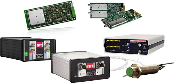
High resolution applications do not always require an interferometer. If you want to make accurate measurements in the micron to picometer range, then an MTI Digital Accumeasure D100 HD or D200 system may be what you need. Laser interferometers can sell for more than $15,000 and be difficult to setup. For example, you may have to buy additional optics to guarantee a good return signal since the laser beam must reflect off a mirror surface or precision retro reflector in order for the beam to re-enter the interferometer’s optics at less than a degree of reflection angle. The downsides [...]