 Power Analyzers: The Backbone of Modern Electrical Engineering Gallery
Power Analyzers: The Backbone of Modern Electrical Engineering
Brand-Vitrek, Industry-Automotive, Industry-Compliance Testing, Industry-Consumer Products, Industry-Energy, Industry-Manufacturing, Industry-Medical, Industry-Medical, Industry-OEM, Industry-R&D, Industry-Semiconductor, News-All Brands, Products-Vitrek-Power-Analyzer, Whitepapers-Vitrek
Power Analyzers: The Backbone of Modern Electrical Engineering
Introduction In the fast-paced world of electrical engineering, ensuring accurate power measurement is crucial for efficiency, reliability, and compliance. Power analyzers play a key role in industries ranging from renewable energy to semiconductor manufacturing, providing engineers with the insights needed to optimize performance and troubleshoot electrical systems. At the forefront of this technology is Vitrek, a leading provider of high-accuracy power analyzers designed for demanding applications. The Role of Power Analyzers in Engineering Power analyzers measure critical electrical parameters such as voltage, current, power factor, and harmonic distortion. Unlike basic meters, these advanced instruments offer high precision measurements over [...]

Precision Control in Semiconductor Wafer Lapping
Application Overview Wafer lapping is a critical semiconductor thinning process that demands tight control to avoid over-removal of material, which can lead to costly yield loss. This application note details how MTI Instruments’ Accumeasure™ capacitive sensing technology enabled precise, real-time displacement and thickness measurement during lapping operations, ensuring consistent wafer quality. Challenge During lapping, wafers are thinned from the backside using a rotating abrasive surface. As the process proceeds, precise feedback is essential to monitor how much material is removed and to determine the wafer's final thickness. Traditional mechanical methods or visual inspections are not sensitive or fast enough [...]
Semiconductor Review: Vitrek Awarded Top Semiconductor Solutions Provider of 2024
Vitrek High-Accuracy Measurement Tools from Silicon to Final Solution Vitrek makes test and measurement solutions for everything from processors to power chips. The company’s broad industry presence is, in part, by design. Vitrek is the union of three complementary companies. Each delivers unique high-precision solutions: MTI Instruments delivers high-precision, non-contact, capacitive measurement tools. GaGe specializes in high-resolution, high-speed digitizer cards. Vitrek, now the parent brand, is renowned for precise hi-voltage measurement products. “Before being merged, each of our companies had established a presence in the industry, addressing the need for high precision in unique ways [...]

High Precision Portable Signal Generators and Calibrators: Everything You Need to Know
High precision portable signal generators are portable electronic devices that generate highly precise signals for testing, system calibration, sensor simulation, troubleshooting, and monitoring. Unlike the benchtop signal generators that are used in laboratories, these hand-held portable devices are designed to be used in the field. The best high precision portable signal generators are also rugged and NIST traceable, meaning that their manufacturer calibrates them to standards from the National Institute of Standards and Technology (NIST). In terms of cost, high precision portable signal generators are more expensive than less precise, lower-end devices that can be held in the hand; [...]
 Did You Know? GaGe RazorMax Express Digitizer/Oscilloscope: An Efficient & Cost-Effective Tool for High-Energy Physics Particle Counting Applications Gallery
Did You Know? GaGe RazorMax Express Digitizer/Oscilloscope: An Efficient & Cost-Effective Tool for High-Energy Physics Particle Counting Applications
Brand-GaGe, Industry-Government/Military, Industry-Measurement Applications, Industry-Medical, Industry-R&D, Industry-Semiconductor, Industry-Semiconductor-GaGe, Knowledge Center-GaGe, Whitepapers-GaGe
Did You Know? GaGe RazorMax Express Digitizer/Oscilloscope: An Efficient & Cost-Effective Tool for High-Energy Physics Particle Counting Applications
Introduction Figure 1. Examples of photo-mulitiplier tubes, or PMTs (Photo courtesy of Hamamatsu). An important category of experimental physics is nuclear and particle physics, a near synonym for high-energy physics. A broad range of experiments in this domain are classed as scattering experiments in which an incident particle hits a target and the resulting scattered particles are studied. Scattering processes can involve the creation or annihilation of particles. The modern approach to studying scattered particles is to employ particle detectors, devices that detect individual particles impinging upon them. This paper provides an overview of typical instruments [...]
 Article: High-Performance Digitizers in Semiconductor Manufacturing Applications Gallery
Article: High-Performance Digitizers in Semiconductor Manufacturing Applications
Application Notes-GaGe, Articles-GaGe, Industry-Compliance Testing, Industry-Semiconductor, Industry-Semiconductor-GaGe, Knowledge Center-GaGe, News-GaGe, News-Industry, Whitepapers-GaGe

Article: High-Performance Digitizers in Semiconductor Manufacturing Applications
High-Performance Digitizers in Semiconductor Manufacturing Applications PC-based high-speed, high-resolution digitizers perform critical data acquisition functions during semiconductor fabrication, die packaging, and final chip testing. Introduction Data acquisition is a critical element of quality control and compliance testing during three stages of semiconductor manufacture. The first stage is fabrication, in which single-crystal semiconductor wafers are subject to various operations that leave them imprinted with micro-circuitry patterns. During the second stage, the wafers are diced up into individual silicon “die” that are packaged into final chips. The third stage involves functional testing of the final chips to [...]
 Press Release: Vitrek Supports the Semiconductor Industry’s Urgent Demand for High-Performance Test Equipment Driven by the CHIPS and Science Act Gallery
Press Release: Vitrek Supports the Semiconductor Industry’s Urgent Demand for High-Performance Test Equipment Driven by the CHIPS and Science Act
Brand-GaGe, Brand-MTI, Brand-Vitrek, Brands-All, Industry-Manufacturing, Industry-Semiconductor, Industry-Semiconductor-Vitrek, New & Press Releases, News-All Brands, News-Events, News-GaGe, News-Industry, News-MTI, News-Vitrek, Press Releases-Vitrek
Press Release: Vitrek Supports the Semiconductor Industry’s Urgent Demand for High-Performance Test Equipment Driven by the CHIPS and Science Act
The $52.7 billion legislation passed in 2022 is driving the expansion of US-based semiconductor sector; Vitrek’s product portfolio includes test and data acquisition products essential for advanced R&D and semiconductor manufacturing.
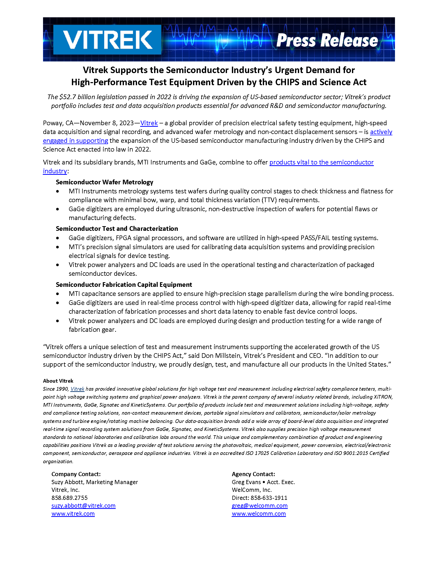
 Video: GaGe Products for the Semiconductor Industry Gallery
Video: GaGe Products for the Semiconductor Industry
Brand-GaGe, Industry-Compliance Testing, Industry-Consumer Products, Industry-Electronics, Industry-Manufacturing, Industry-Measurement Applications, Industry-R&D, Industry-Semiconductor, Industry-Semiconductor-GaGe, Industry-Semiconductor-Videos, Knowledge Center-GaGe, News-GaGe, News-Products, News-Vitrek, Videos-GaGe
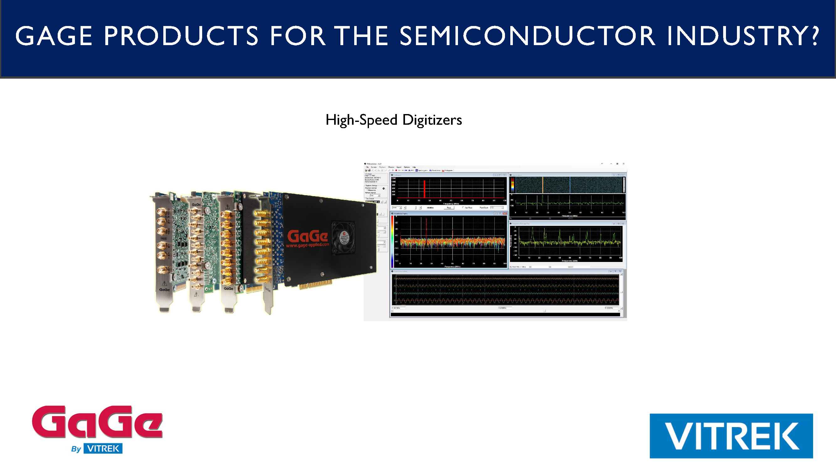
 Video: MTI Products for the Semiconductor Industry Gallery
Video: MTI Products for the Semiconductor Industry
Brand-MTI, Industry-Compliance Testing, Industry-Consumer Products, Industry-Electronics, Industry-Manufacturing, Industry-Measurement Applications, Industry-R&D, Industry-Semiconductor, Industry-Semiconductor-MTI, Industry-Semiconductor-Videos, Knowledge Center-MTI, News-MTI, Videos-MTI, Videos-MTI-Capacitance Sensors, Videos-MTI-Manual Semiconductor Metrology System, Videos-MTI-Semiautomated Metrology System
 MTI Instruments Whitepaper: Capacitance Guide for Industrial Applications Gallery
MTI Instruments Whitepaper: Capacitance Guide for Industrial Applications
Brand-MTI, Industry-Aerospace, Industry-Automotive, Industry-Battery, Industry-Compliance Testing, Industry-Consumer Products, Industry-Electronics, Industry-Energy, Industry-Government/Military, Industry-Industrial Processing, Industry-Lighting, Industry-Manufacturing, Industry-Measurement Applications, Industry-OEM, Industry-R&D, Industry-Semiconductor, Industry-Semiconductor-MTI, Industry-Sensors, Industry: Transportation, Knowledge Center-MTI, News-MTI, Whitepapers-MTI
MTI Instruments Whitepaper: Capacitance Guide for Industrial Applications
Capacitance Guide for Industrial Applications This guide from MTI Instruments explains what you need to know about using electrical capacitance for measurement in industrial applications, including advanced manufacturing. Basic Principles Capacitance is the ratio of the change in an electric charge to the corresponding change in its electrical potential (i.e., voltage). Capacitors, components that that have the “capacity” to store an electric charge, consist of conductive parallel plates that don’t touch or connect with each other. Instead, these metal plates are electrically-separated by air or a layer of insulating material (i.e., the dielectric). MTI’s [...]