Introduction
Every semiconductor device begins with a nearly perfect wafer. Yet throughout fabrication, that wafer is repeatedly transformed by dozens of manufacturing processes including thin-film deposition, oxidation, implantation, annealing, polishing, and packaging. While each process is designed to modify the electrical properties of the device, it also alters something far less visible—its mechanical condition.
The addition of every thin film introduces internal mechanical forces that can subtly change the shape of the wafer. These changes, often measured in only a few micrometers across a 200 mm or 300 mm substrate, may appear insignificant. However, as semiconductor devices continue to shrink and manufacturing tolerances become increasingly demanding, even small changes in wafer geometry can influence lithography accuracy, process repeatability, package reliability, and ultimately manufacturing yield.
For many years, wafer stress was considered primarily a research or failure analysis concern. Today, it has become an important production metric. Advanced semiconductor manufacturers increasingly monitor wafer geometry throughout the fabrication process to identify equipment drift, optimize deposition recipes, validate new materials, and improve long-term process stability. Rather than serving solely as a quality inspection tool, stress measurement has evolved into an important element of modern process control.
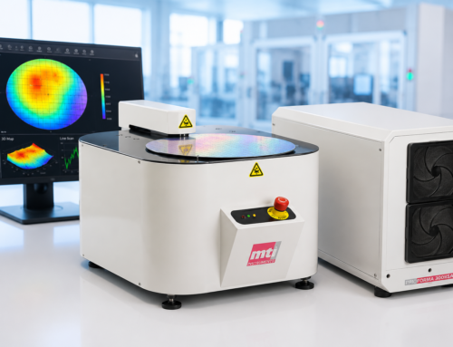
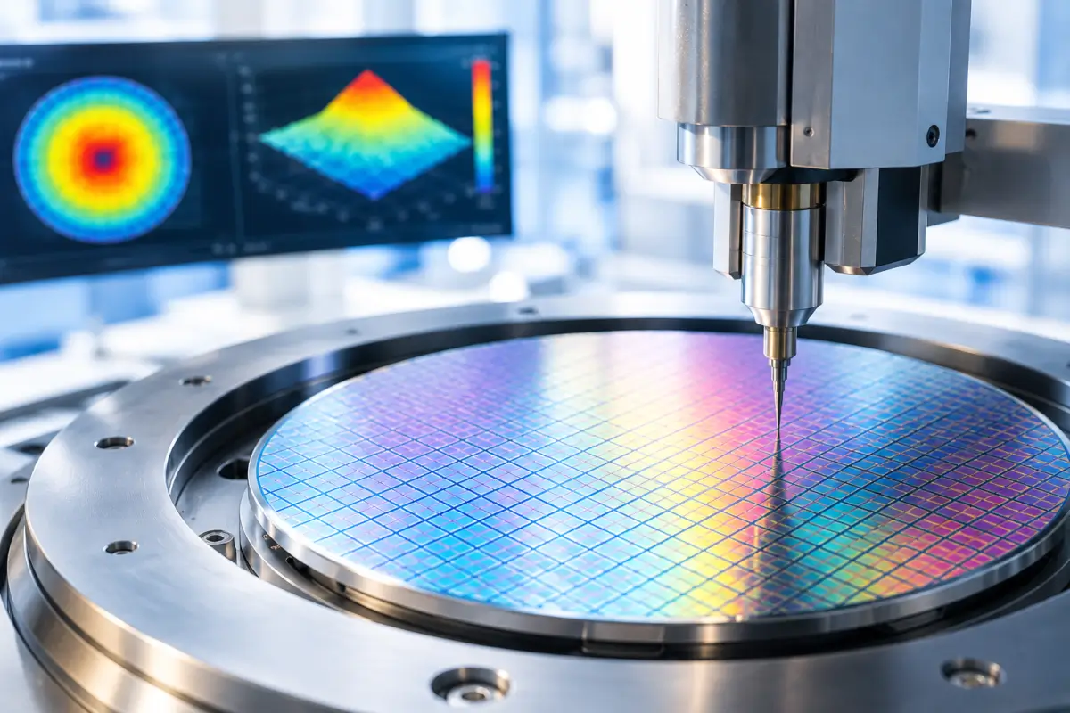
Advances in non-contact metrology have made this transition possible. Modern measurement systems can rapidly characterize the entire wafer surface with exceptional repeatability, providing engineers with a comprehensive view of wafer geometry instead of relying on a limited number of measurement locations. When combined with graphical visualization and quantitative stress analysis, these measurements provide valuable insight into the mechanical behavior of the
manufacturing process itself.
This paper explains the fundamentals of wafer stress, examines how mechanical forces influence semiconductor manufacturing, and explores how full-wafer measurement techniques support process optimization, yield improvement, and production consistency across today’s advanced fabrication environments.
The Hidden Variable in Semiconductor Manufacturing
Modern semiconductor fabrication is often described in terms of electrical performance, feature size, and process precision. Discussions typically focus on transistor density, line widths measured in nanometers, critical dimensions, and increasingly sophisticated device architectures. While these parameters define the functional performance of an integrated circuit, they represent only part of the manufacturing challenge.
Every deposited material possesses its own mechanical properties. As thin films accumulate throughout the manufacturing process, they introduce internal forces that continuously alter the physical shape of the wafer. Because these changes occur gradually—and often remain invisible to the naked eye—they can easily go unnoticed until they begin affecting downstream operations.
A wafer that appears perfectly acceptable after deposition may exhibit enough curvature to influence lithography focus several process steps later. Slight non-uniformity across the substrate may contribute to overlay errors, uneven polishing during chemical mechanical planarization (CMP), or difficulties during wafer bonding and advanced packaging. In other cases, excessive stress can lead to film cracking, delamination, die fracture, or package warpage long after the originating process has been completed.
As device complexity increases, the tolerance for these mechanical variations continues to decrease. Three-dimensional device structures, advanced memory technologies, heterogeneous integration, silicon carbide (SiC), gallium nitride (GaN), MEMS, integrated photonics, and chiplet-based packaging all depend upon exceptional control of wafer geometry throughout manufacturing. Mechanical stability has become just as important as electrical performance.
Understanding how stress develops—and how it changes throughout fabrication—is an essential part of semiconductor process engineering. The goal is not simply to measure wafers. The goal is to understand the mechanical condition of the manufacturing process itself.
Understanding Thin Film Stress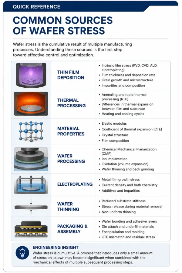
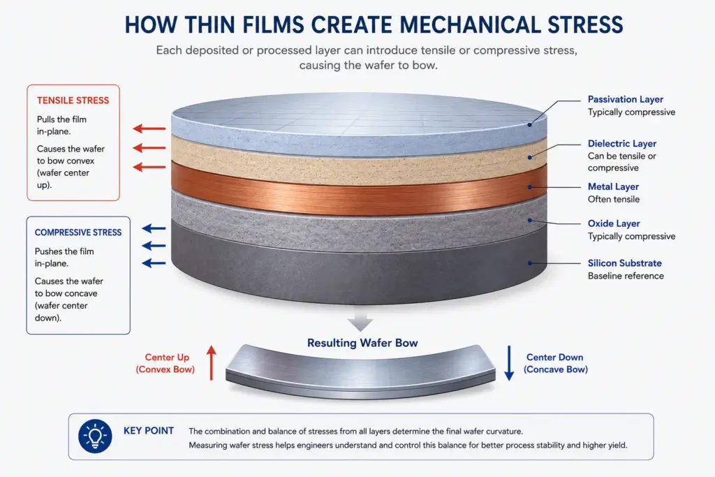
Every thin film deposited during semiconductor manufacturing introduces some degree of mechanical stress into the underlying substrate. Whether the objective is to create an insulating dielectric, a conductive metal layer, a barrier film, or a protective coating, the deposited material possesses physical properties that differ from those of the silicon wafer beneath it. As these materials bond together, internal mechanical forces develop naturally.
Stress itself is neither unusual nor inherently undesirable. In fact, every successful semiconductor manufacturing process operates with some level of residual stress. The objective is not to eliminate stress entirely, but to understand how it develops, monitor how it changes throughout fabrication, and maintain it within a predictable operating window.
When stress remains stable and repeatable, manufacturing processes generally produce consistent results. When stress begins to change unexpectedly, it often provides one of the earliest indicators that a process is drifting out of specification.
Sources of Wafer Stress
Wafer stress develops throughout semiconductor manufacturing as thin films are deposited, materials are heated and cooled, and subsequent process steps alter the wafer’s mechanical condition. Although these sources are often discussed separately, the final stress profile typically reflects the combined effects of multiple manufacturing operations.
Intrinsic Film Stress – Develops naturally during thin-film deposition.
Thermal Stress – Results from thermal expansion mismatch between the film and substrate.
Process-Induced Stress – Introduced during processes such as CMP, implantation, and packaging.
Regardless of their origin, these stress mechanisms ultimately influence wafer geometry and determine how the wafer responds during subsequent manufacturing processes.
Tensile & Compressive Stress
Regardless of how wafer stress is introduced, its mechanical effects are generally classified as either tensile or compressive. These two stress states determine how the wafer responds to the forces generated during fabrication and provide a common framework for evaluating thin-film behavior.
Tensile Stress – Tensile stress occurs when a deposited film tends to contract relative to the substrate, placing the wafer surface under tension. If excessive, tensile stress can contribute to film cracking, delamination, and reduced long-term reliability.
Compressive Stress – Compressive stress occurs when a deposited film tends to expand relative to the substrate, pushing against the wafer surface. High compressive stress can increase wafer bow, promote film buckling, and create challenges during downstream handling and packaging.
Neither stress state is inherently better than the other. Most semiconductor manufacturing processes are designed to operate within a controlled stress window, where mechanical forces remain predictable and repeatable. The objective is not to eliminate stress, but to maintain a stable balance that preserves wafer geometry and supports consistent manufacturing performance.
From Mechanical Forces to Manufacturing Performance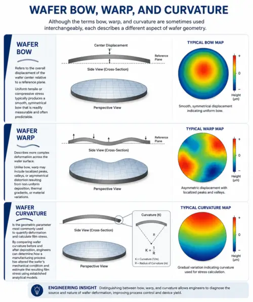
Although stress originates at the atomic level, its effects extend throughout the manufacturing process.
A slight increase in wafer curvature may influence lithography focus during subsequent process steps. Small changes in stress distribution can affect polishing uniformity, wafer handling, die singulation, and advanced packaging operations. Because these effects accumulate over multiple fabrication stages, the source of the problem may be separated by days—or even weeks—from the point at which the failure is ultimately observed.
For this reason, wafer stress is increasingly viewed as a leading indicator of process health rather than another quality measurement. By monitoring changes in wafer geometry throughout production, manufacturers gain valuable insight into equipment performance, recipe stability, and long-term process consistency before yield losses begin to occur.
Wafer Bow, Warp & Curvature
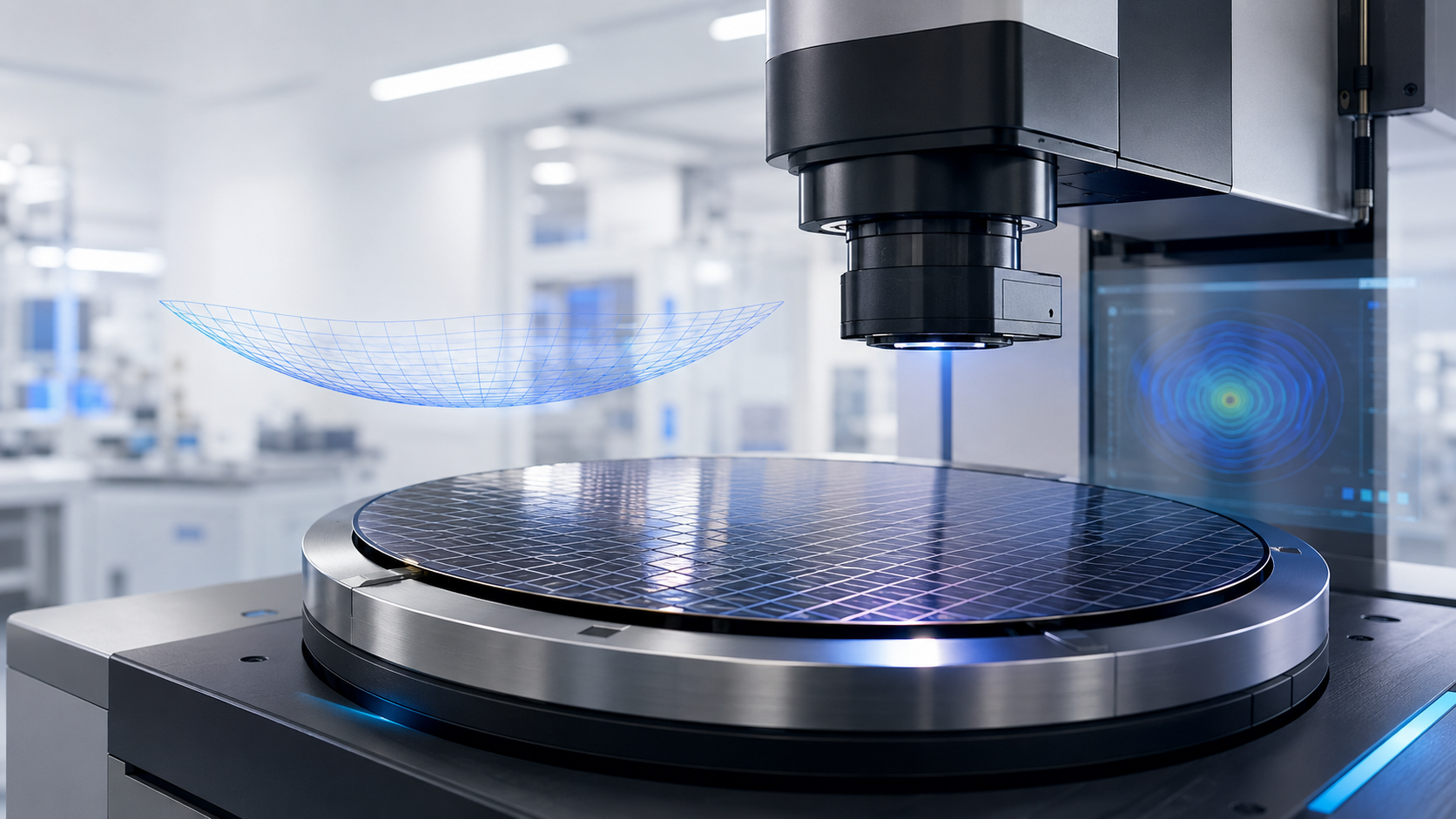
The mechanical effects of wafer stress are most commonly observed through changes in wafer geometry. As thin films are deposited and manufacturing processes progress, internal stresses can cause the wafer to deform in different ways depending on the magnitude and distribution of those forces. While the terms bow, warp, and curvature are often used interchangeably, each describes a distinct characteristic of wafer deformation and provides engineers with valuable insight into process stability and film behavior. Understanding these differences is essential for accurately interpreting measurement data, identifying process variation, and optimizing semiconductor manufacturing.
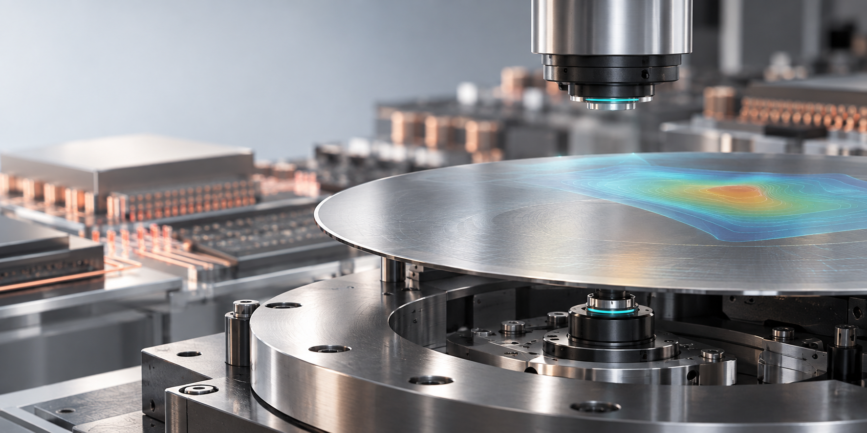
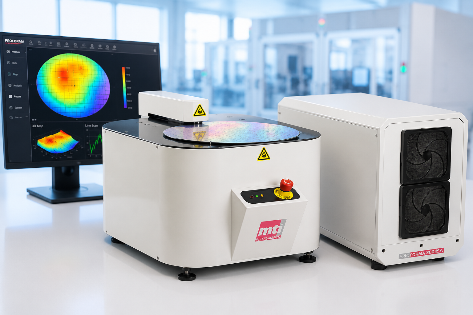
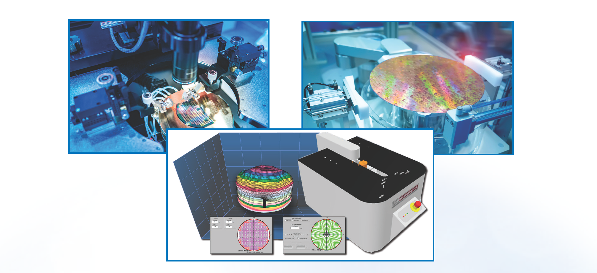
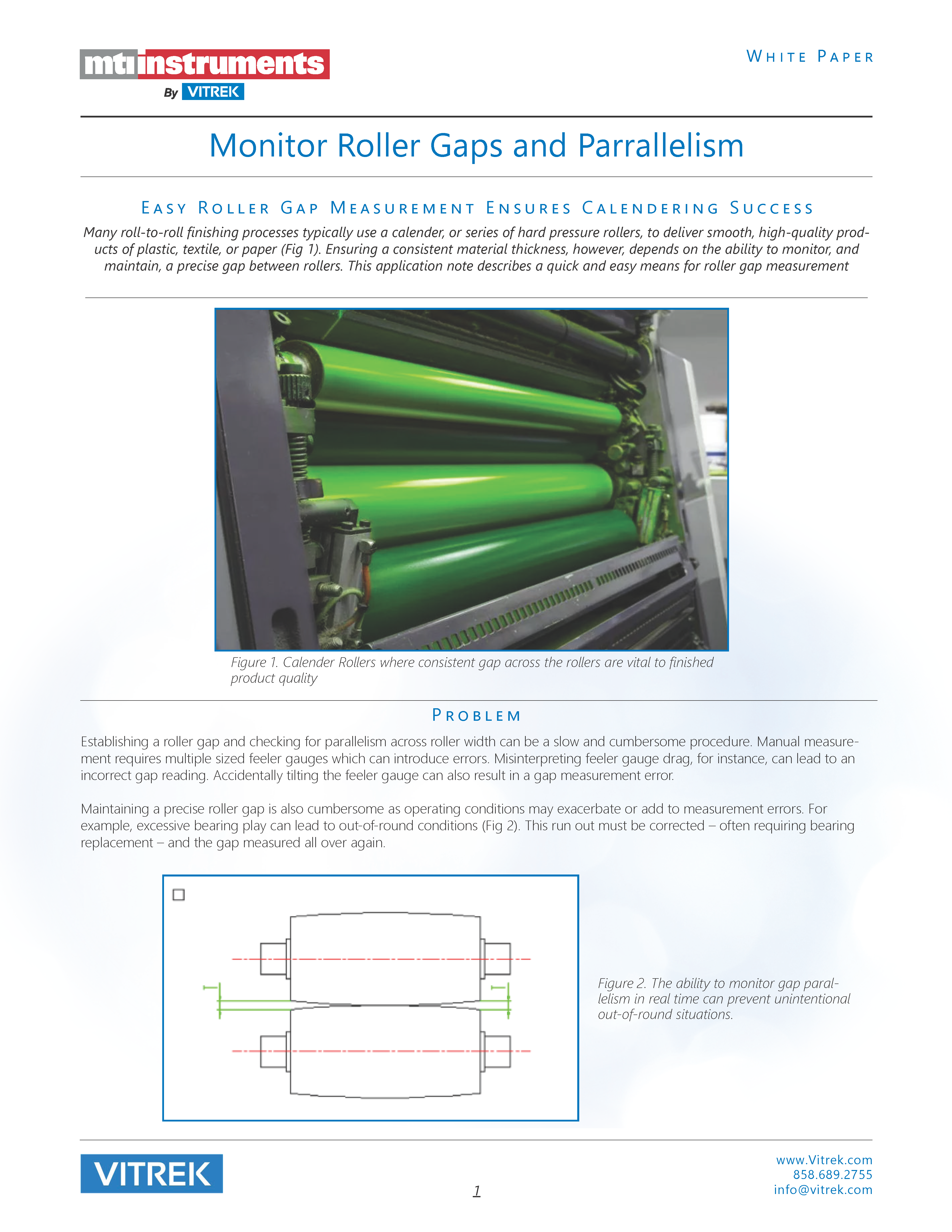
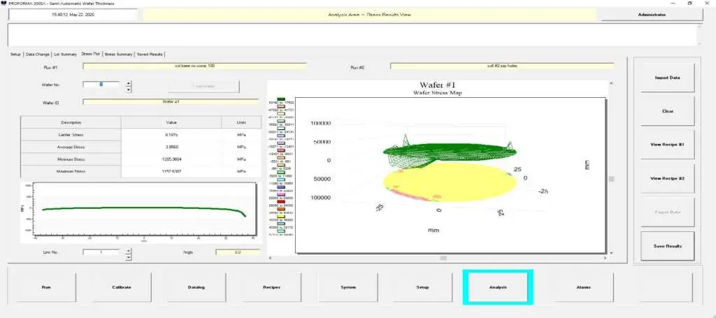
Modern full-wafer measurement techniques capture thousands of data points across the entire substrate, producing a comprehensive representation of wafer geometry. Rather than relying on a single numerical value, engineers can visualize how stress is distributed from the center of the wafer to its edge, revealing subtle patterns that may indicate equipment drift, thermal imbalance, or deposition non-uniformity.
This holistic view allows process engineers to identify trends that would otherwise remain hidden and provides valuable context for optimizing manufacturing processes.
Why Full Wafer Measurement Matters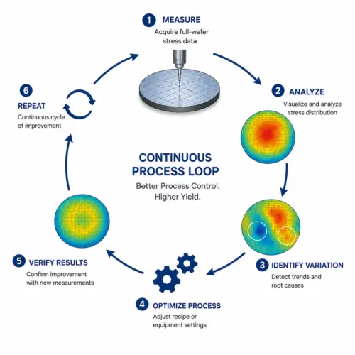
Historically, wafer geometry was often evaluated using measurements taken at only a limited number of locations. While these methods provided useful information about overall flatness, they frequently overlooked localized variations that could significantly influence downstream manufacturing.
Modern full-wafer measurement techniques capture thousands of data points across the entire substrate, producing a comprehensive representation of wafer geometry. Rather than relying on a single numerical value, engineers can visualize how stress is distributed from the center of the wafer to its edge, revealing subtle patterns that may indicate equipment drift, thermal imbalance, or deposition non-uniformity.
This holistic view allows process engineers to identify trends that would otherwise remain hidden and provides valuable context for optimizing manufacturing processes.
From Measurement to Process Control
Collecting accurate wafer stress data is only the beginning. The greatest value lies in transforming those measurements into actionable process information that supports continuous manufacturing improvement.
Rather than evaluating individual wafers in isolation, engineers increasingly trend stress measurements across production lots to monitor process stability over time. Small changes in stress distribution may indicate chamber contamination, target wear, thermal drift, equipment maintenance requirements, or material variation long before defects become apparent through electrical testing or final inspection.
When combined with statistical process control (SPC) techniques, wafer stress measurements become a powerful indicator of manufacturing health. Engineers can establish baseline stress profiles, monitor process capability, verify recipe changes, and quickly identify deviations that require investigation. This proactive approach helps reduce process variability, improve yield, and shorten the time required to diagnose manufacturing issues.
The objective is no longer simply to measure wafer stress—it is to use stress data as part of a continuous improvement strategy that supports stable, repeatable semiconductor manufacturing.
Using Wafer Stress to Improve Manufacturing
Measuring wafer stress is only the first step. The true value lies in transforming measurement data into actionable process insight. By monitoring wafer stress throughout fabrication, engineers gain early vis-ibility into process stability, equipment performance, and material behavior before defects appear during inspection or electrical testing.
Rather than evaluating individual wafers, manufacturers trend stress measurements across production lots to establish performance baselines and monitor long-term consistency. Changes in stress distribution can reveal chamber contamination, thermal drift, material variation, or recipe instability, enabling correc-tive action before yield or reliability is affected.
As semiconductor technologies continue to advance, controlling mechanical behavior has become as im-portant as controlling electrical performance. Wafer stress measurement is now an essential component of modern process control, helping manufacturers optimize processes, improve repeatability, increase yield, and support continuous manufacturing improvement.
Engineering Applications
Monitor Process Stability – Trend wafer stress to verify process consistency and detect early drift.
Detect Equipment Drift – Identify chamber, thermal, or equipment changes before they affect yield.
Optimize Thin-Film Deposition – Compare recipes to improve film stress and wafer geometry.
Validate Process Changes – Measure the impact of new materials, recipes, or maintenance activities.
Support Statistical Process Control (SPC) – Establish baselines, monitor trends, and enable early corrective action.
Improve Manufacturing Yield – Reduce stress-related variation that impacts yield and reliability.
Accelerate Process Development – Shorten process optimization and qualification cycles with objective data.
Enhance Product Reliability – Maintain consistent mechanical behavior for improved long-term reliability.
Conclusion
Wafer stress is an inherent part of semiconductor manufacturing, but when properly understood and monitored, it becomes a valuable indicator of process health rather than simply a mechanical measure-ment. By characterizing wafer geometry throughout fabrication, engineers can detect process variation earlier, optimize manufacturing conditions, improve yield, and support long-term device reliability. As semiconductor technologies continue to evolve, understanding wafer stress will remain essential for achieving consistent, repeatable, and efficient manufacturing performance.