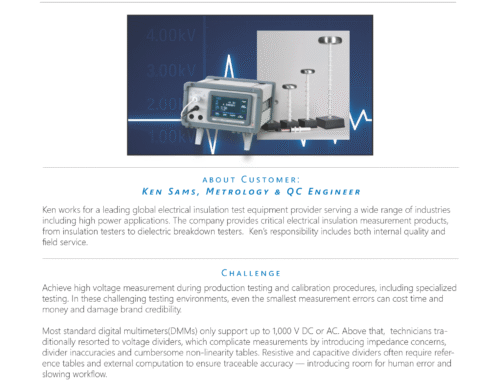
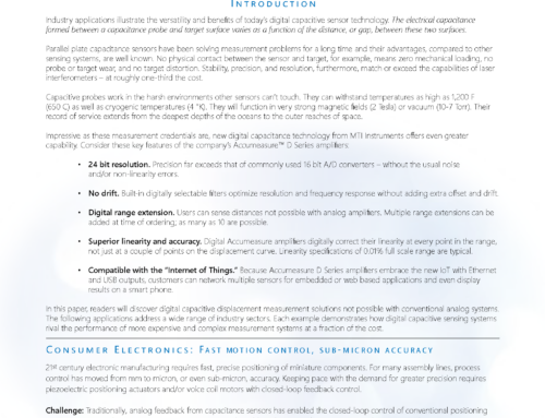
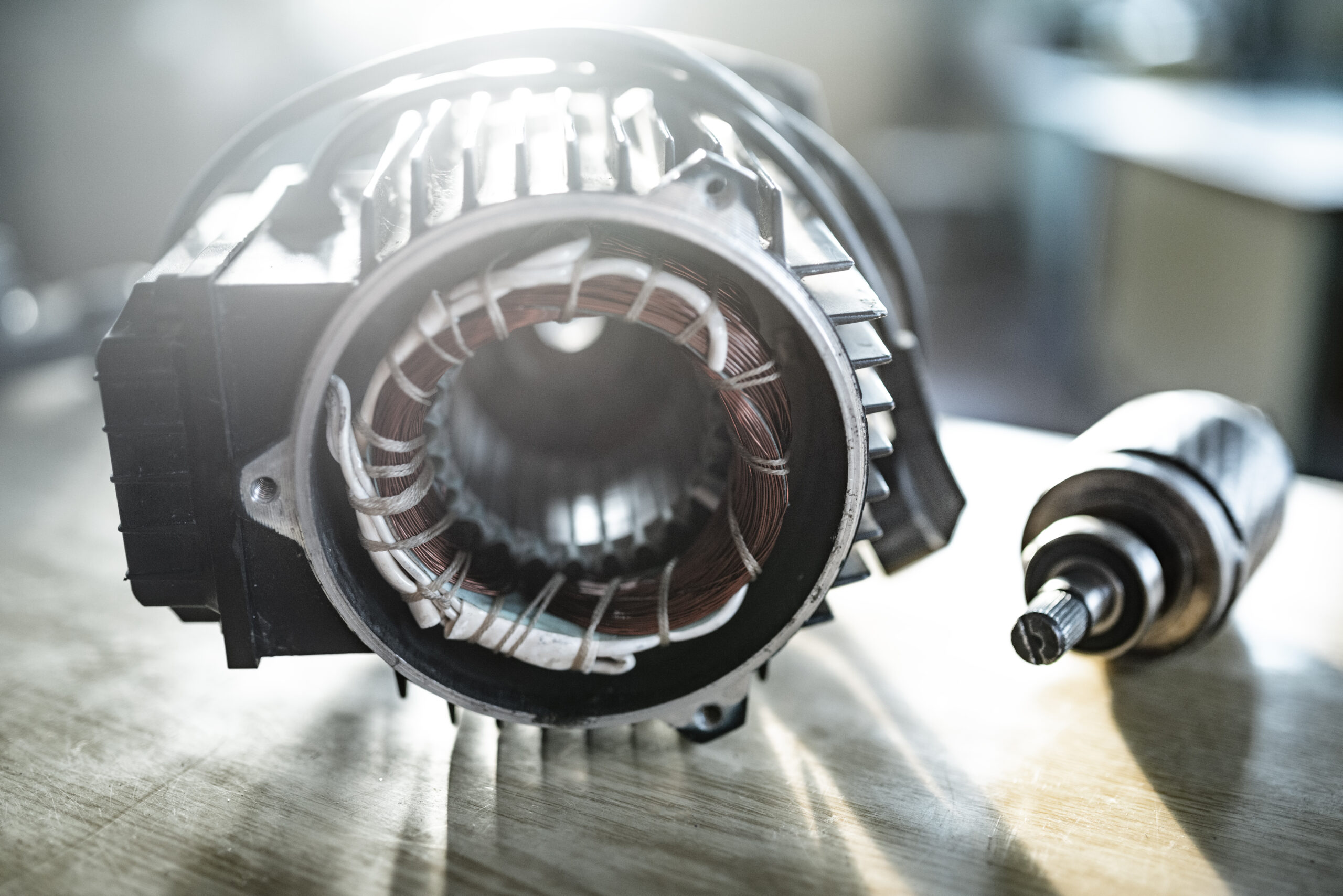
Remember that old acronym, GIGO? Garbage in garbage out, it can apply to raw materials as well as programming. Sapphire wafers need to be of a certain quality to ensure maximum yield.
-
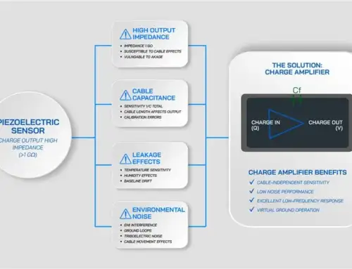
EXCESSIVE TTV, BOW, AND WARP LEAD TO PREMATURE LED FAILURE
-
LED MANUFACTURERS NEED TO INSPECT INCOMING WAFERS.
-
WAFER PRODUCERS ALSO NEED TO CHECK AND CONTROL TTV, BOW AND WARP.
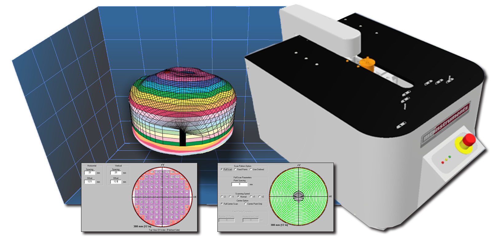
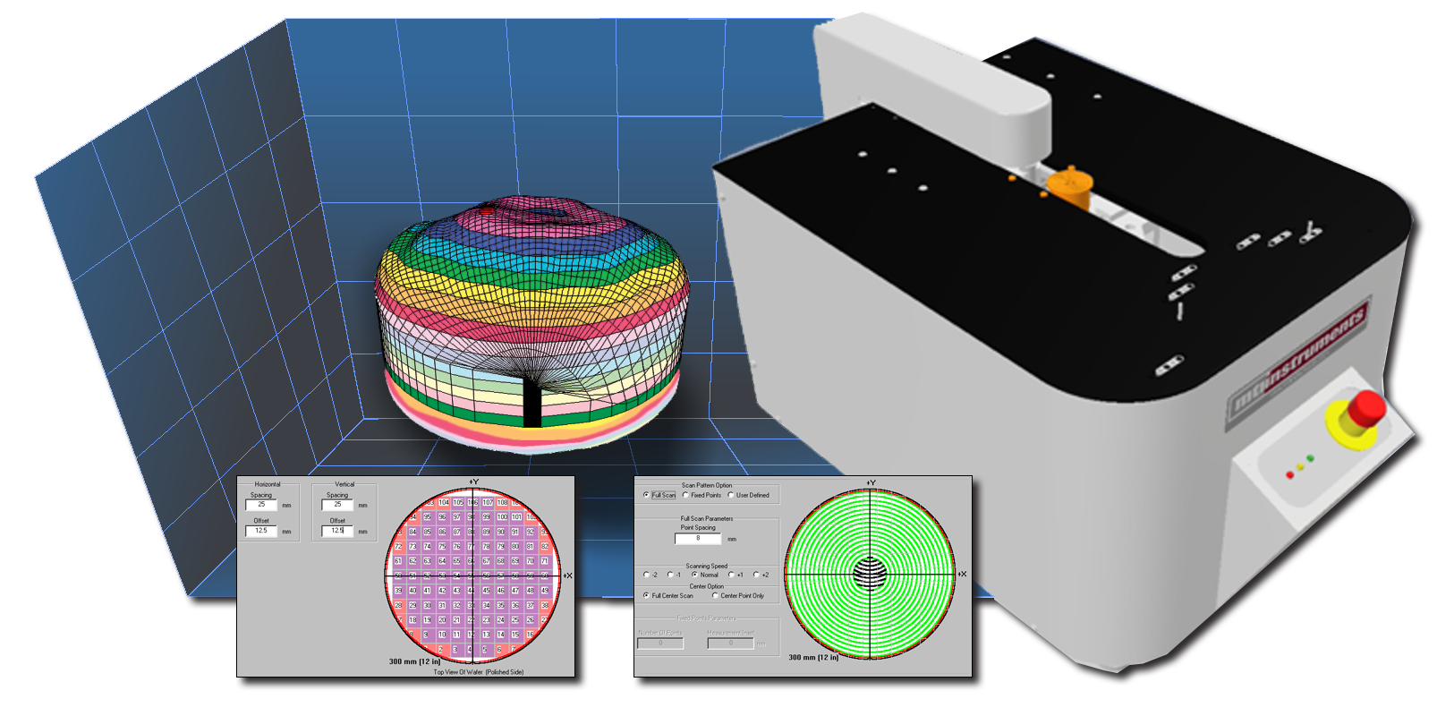
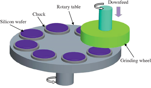
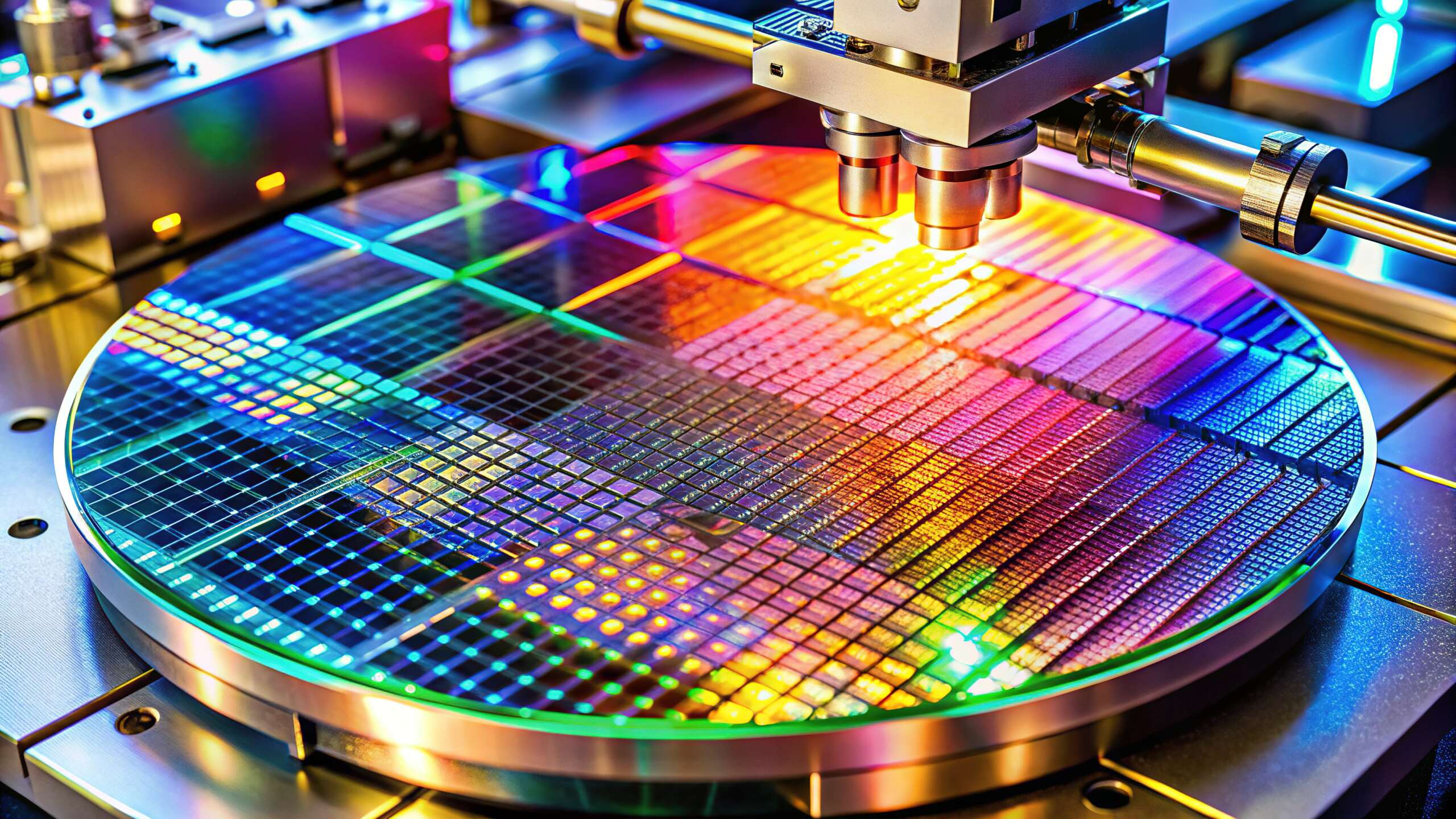
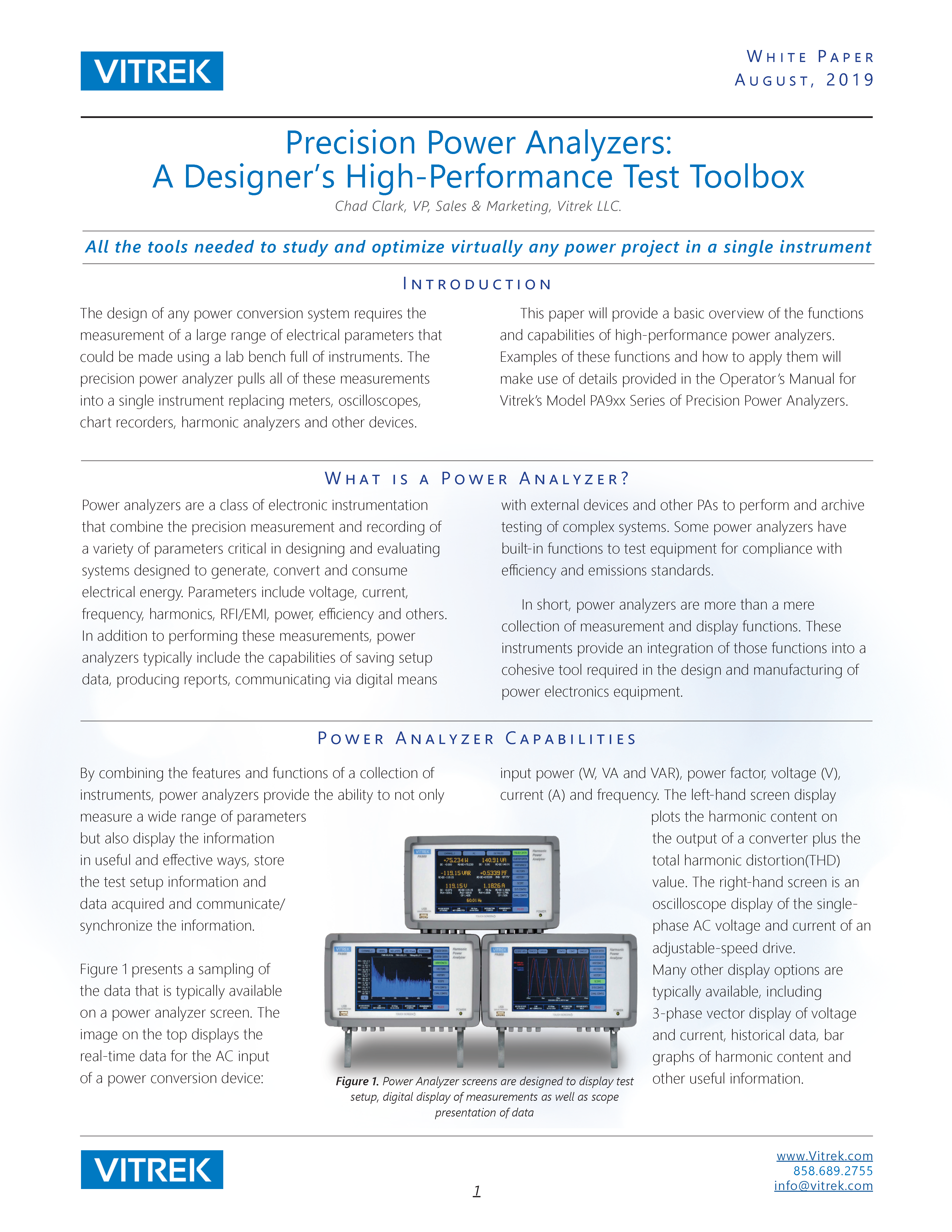
The market for sapphire wafers, driven by the growth in LED manufacturing, is booming. While the price has come down significantly since 2011, the size of the wafers has increased dramatically from 2 inches to 6 inch and beyond. The increase in size introduces more probability of significant total thickness variation (TTV), Bow and Warp.
 |
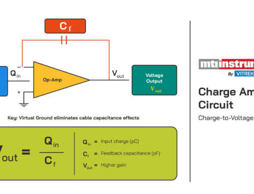
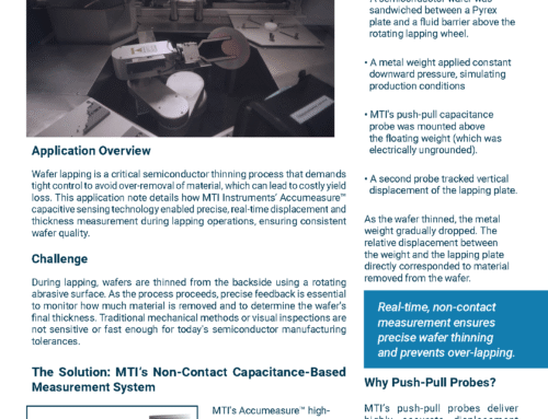
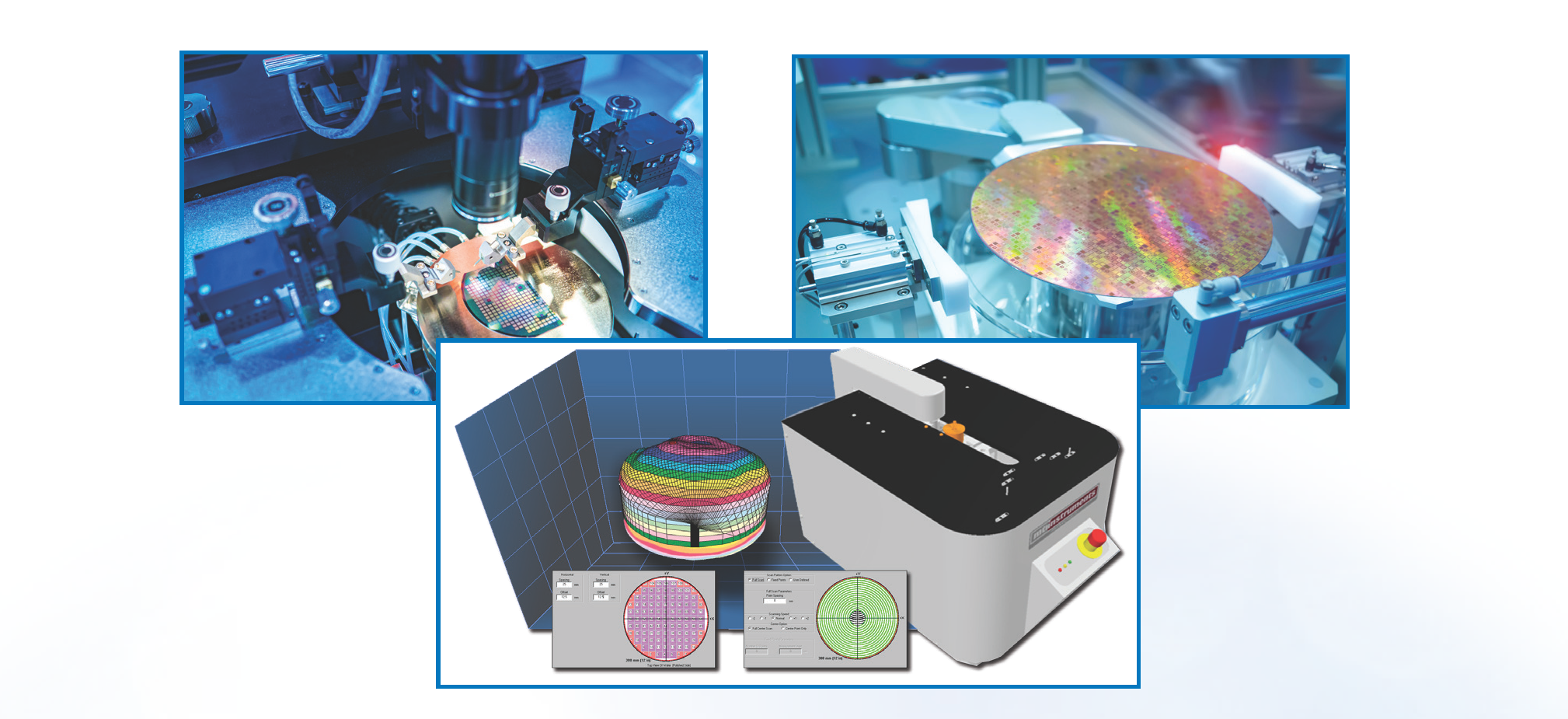
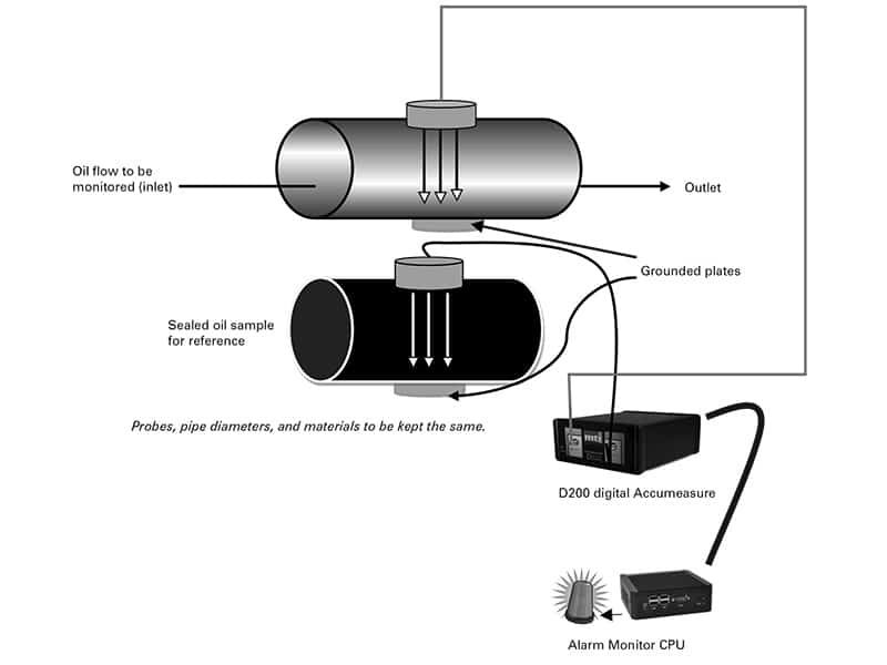
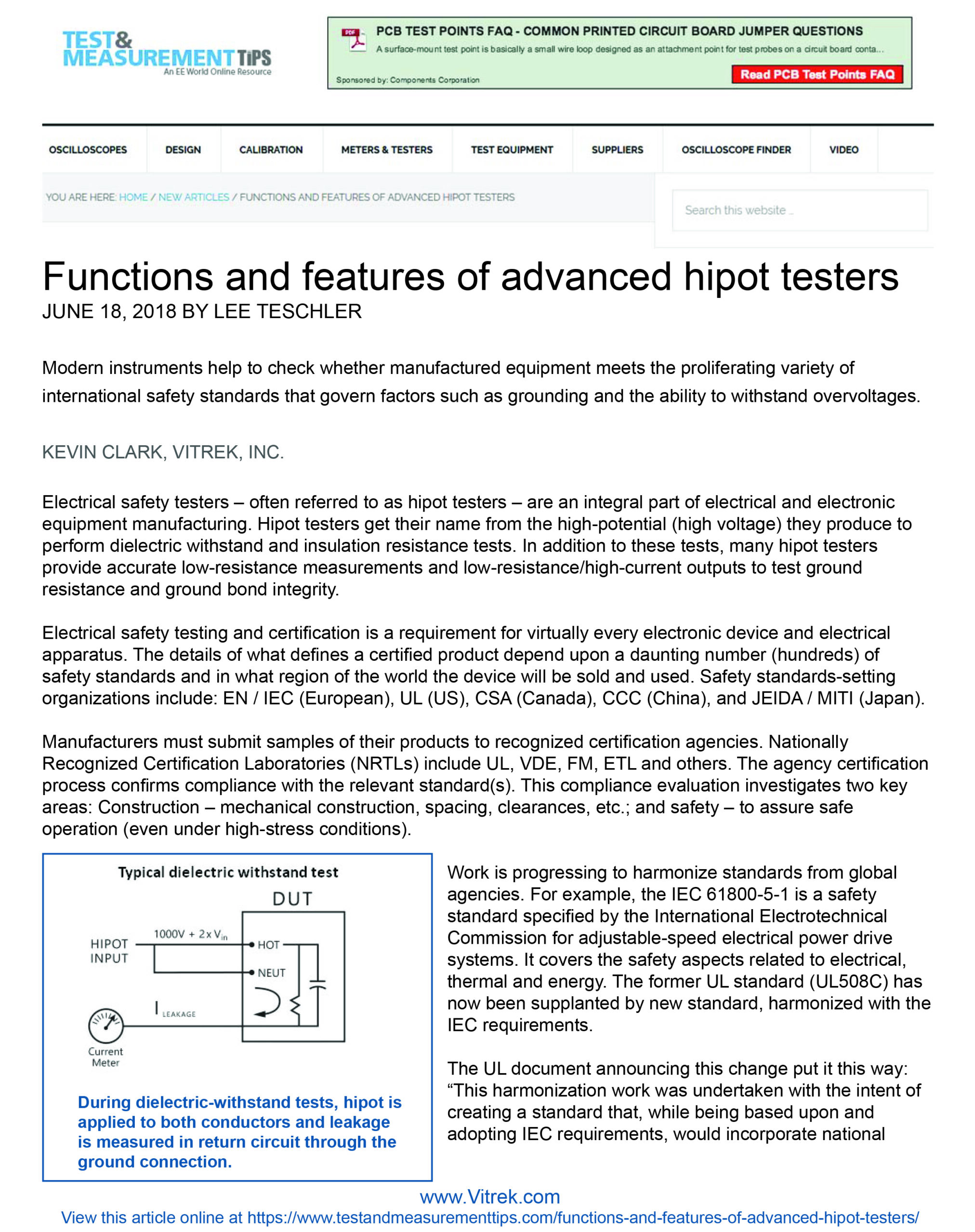
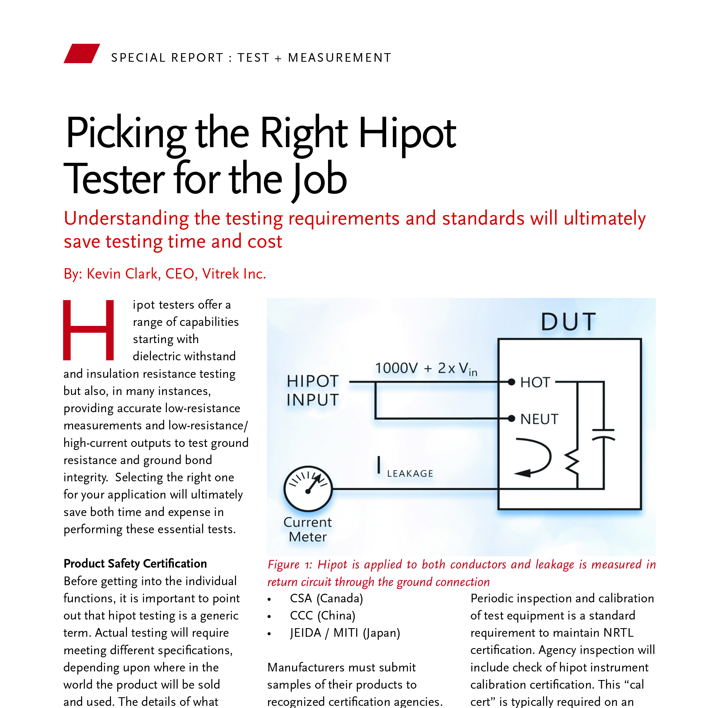
PLACING A DIELECTRIC (NON-CONDUCTING) MATERIAL BETWEEN A CAPACITANCE PROBE AND A GROUND PLANE CREATES A CAPACITIVE CIRCUIT THAT CAN BE ANALYZED TO DETERMINE TOTAL THICKNESS. |
Set up is quick and easy, simply determine the range limit of the probe (by adjusting the height until the indicator on the amplifier just turns green) and entering zero in the first sample thickness, press calibrate, and then place a wafer of known thickness between the probe and ground plane. Now enter the known thickness into the second sample thickness and calibrate the second sample. This has stored the dielectric constant which will be used to measure all remaining wafers.
 |
 |
| Insert a wafer of unknown thickness. The thickness of the wafer is displayed in the upper left corner. |
 |
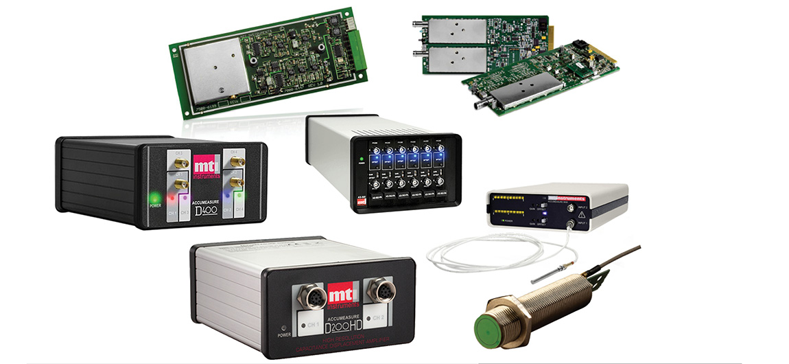
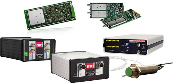
WHAT YOU NEED:
-
DIGITAL ACCUMEASURE TM CAPACITANCE AMPLIFIER
-
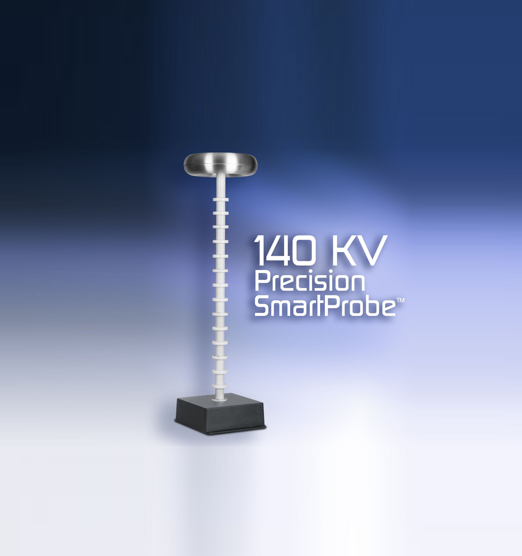
D100 OR D110 CAPACITANCE PROBE
-
DIELECTRIC FIXTURE
-
24VDC POWER SUPPLY
-
MICRO USB CABLE
-
LAPTOP OR DESKTOP COMPUTER
The AccumeasureTM D Measurements program is included with the Purchase of the AccumeasureTM D series Capacitance Amplifier.
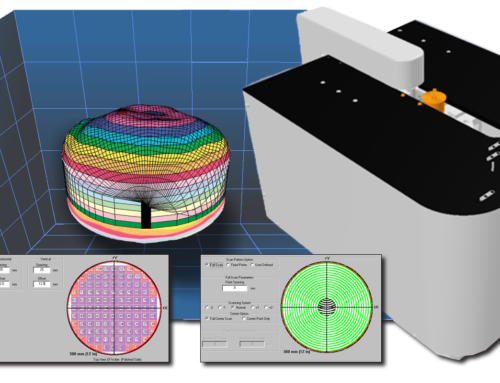
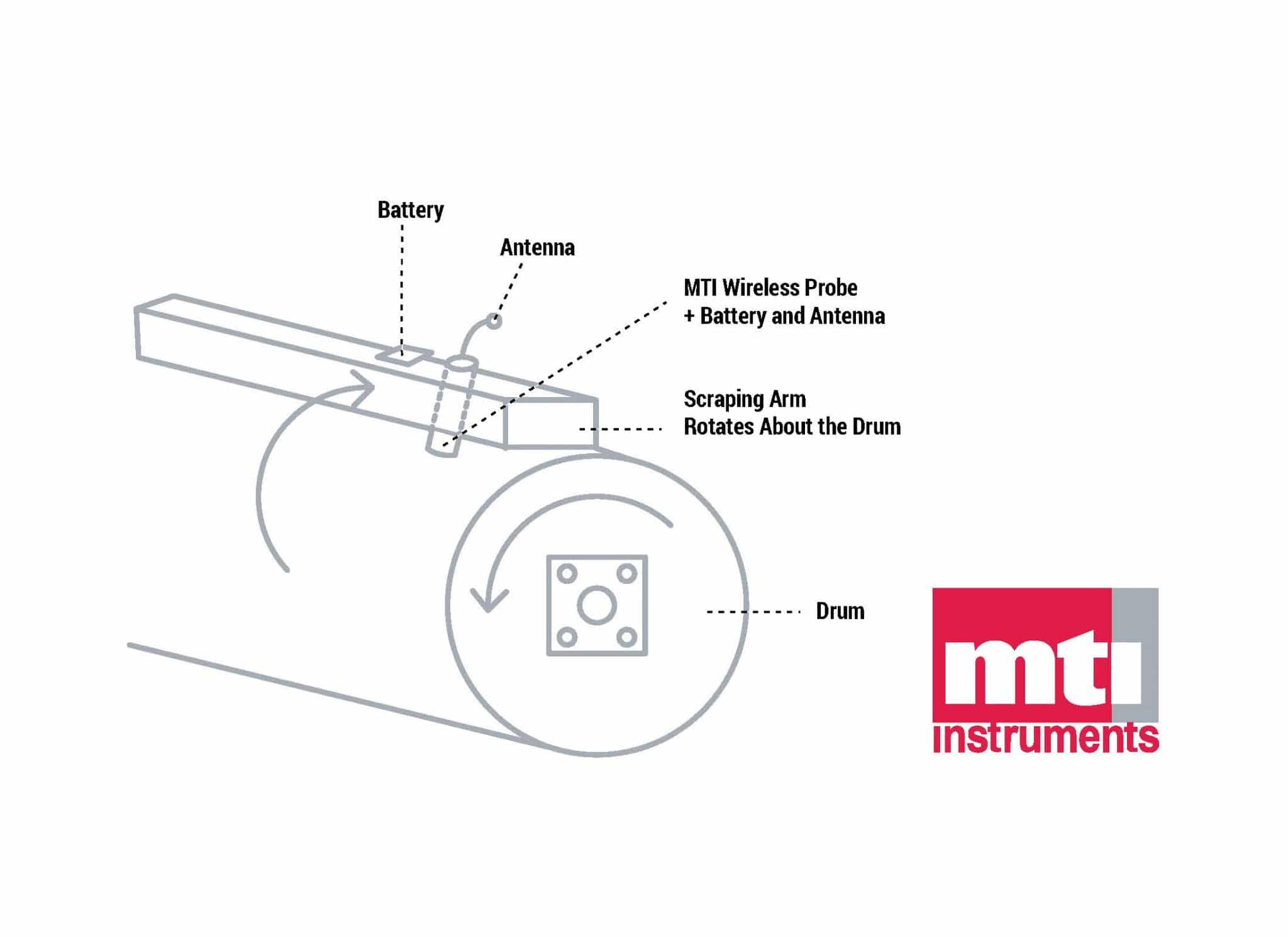
For measuring bow and warp.
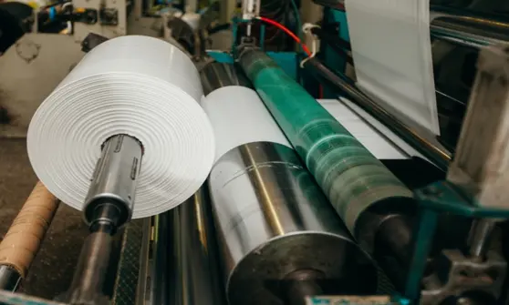
Establish a precision three point reference plane to hold the wafer and then subtract the wafer thickness from the height of the three point plane to calculate bow and warp. See MTI’s App note for how to calculate wafer measurements. The Digital AccumeasureTM Capacitance Amplifier is also perfect for measuring other non-conductive commodities such as Plastic, Glass, Optical Disc’s, Paper, Plastic and Rubber. MTI Instruments, Inc. offers several styles and types of non-contact sensors that can be customized to your exact requirements. If you have a difficult application to solve, contact our experienced team of application engineers¬†who will thoroughly analyze your requirements and guide you to a practical, cost-effective solution.


