
Introduction
Artificial intelligence and high-performance computing are reshaping semiconductor design and manufacturing. Instead of relying exclusively on increasingly large monolithic devices, manufacturers are integrating logic, memory and specialized functions through chiplets, 2.5D packaging, 3D stacking and high-bandwidth memory.
These architectures improve computing density, bandwidth and energy efficiency, but they also place greater demands on wafer thinning and backside processing. Individual wafers and dies may need to be made significantly thinner before stacking, bonding or package assembly. As thickness decreases, however, wafers become more susceptible to breakage, warpage, handling damage and non-uniform material removal.
Thickness metrology therefore becomes more than a final inspection step. It provides process information that manufacturers can use to identify drift, evaluate grinding and polishing performance, and prevent unsuitable wafers from advancing into costly downstream packaging operations.
Why Advanced Packaging Changes the Measurement Challenge
Advanced packaging combines multiple components into a tightly integrated structure. These may include logic dies, HBM stacks, interposers, redistribution layers and other specialized devices.
The resulting package must meet demanding requirements for physical height, alignment, thermal behavior and mechanical stability. Wafer and die thickness can affect each of these factors.
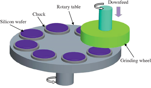
Backside grinding reduces the bulk thickness of the wafer. Fine grinding, polishing or stress-relief processes may then be used to remove subsurface damage and prepare the wafer for subsequent operations. Manufacturers must control not only average thickness, but also total thickness variation and wafer shape.
If too much material is removed, the wafer may become difficult to handle or unsuitable for the intended package. If material removal is uneven, local thickness variations can complicate bonding, stacking and assembly. Bow and warp may also increase as the wafer becomes thinner or as films and other materials create mechanical stress.
For high-value AI and advanced-memory devices, these problems can become especially costly because substantial value may already have been added before the wafer reaches the packaging line.
Thickness Data as a Process-Control Tool
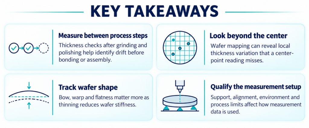
A single final measurement cannot reveal when a thinning process began to drift. Measurements taken at defined checkpoints provide more useful information.
For example, engineers may inspect wafers after coarse grinding, fine grinding and polishing.
Comparing data between these stages helps them determine:
- Whether material is being removed at the expected rate
- Whether thickness variation is increasing or decreasing
- Whether a grinding or polishing process is removing material uniformly
- Whether wafer bow or warp is changing
- Whether the process is approaching an established control limit
Trend data can also reveal gradual changes associated with grinding-wheel wear, fixture condition, process recipes or handling practices.
The objective is not simply to determine whether the final wafer passes inspection. It is to recognize an adverse trend early enough to correct the process before more wafers—and more downstream value—are placed at risk.
Why Non-Contact Measurement Matters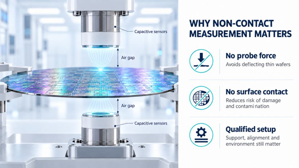
Mechanical contact can present challenges when measuring thin, delicate or high-value wafers. Probe force may deflect the wafer, affect repeatability or introduce a risk of surface damage and contamination.
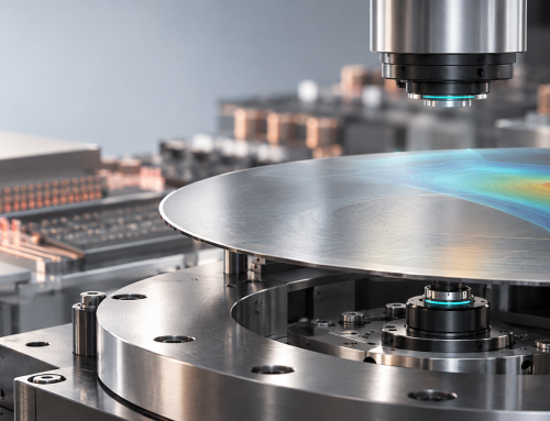
Non-contact measurement avoids applying mechanical force to the wafer surface. When paired with controlled wafer positioning and suitable fixturing, it can provide repeatable thickness data without adding another contact-based handling step.
Measurement performance must still be evaluated as a complete system. Sensor resolution alone does not define measurement accuracy. Fixture stability, sensor alignment, wafer support, cleanliness, temperature, vibration and repeated loading all influence the result.
This distinction becomes increasingly important as process tolerances tighten. A measurement system must be qualified under the actual conditions in which it will be used.
Applying Proforma Metrology to Backside Processing
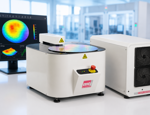
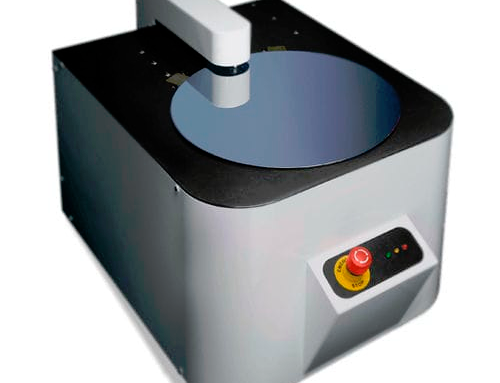
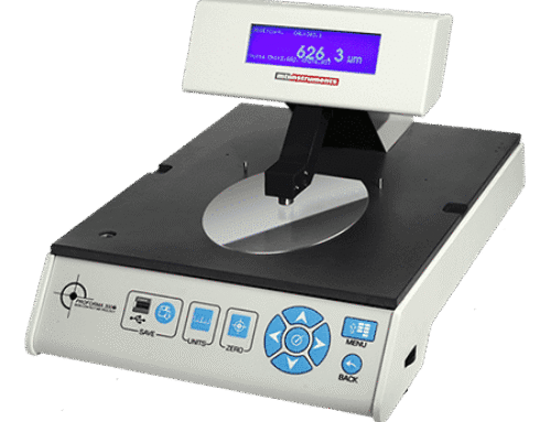
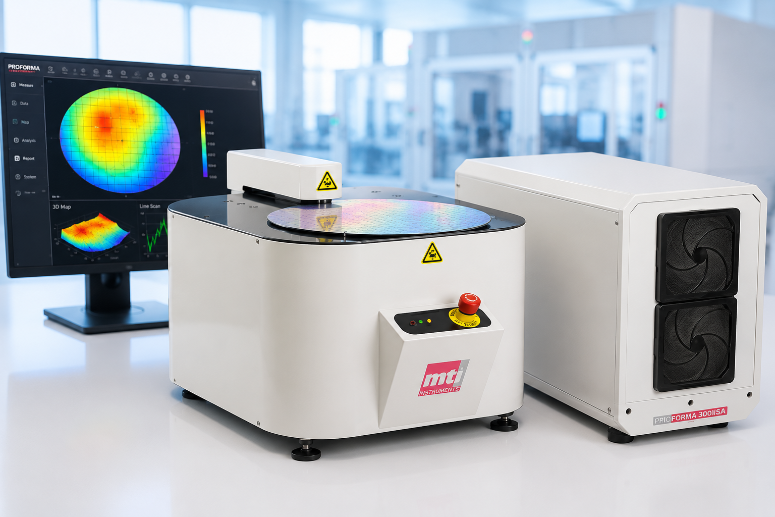
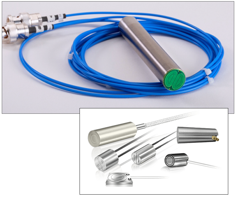
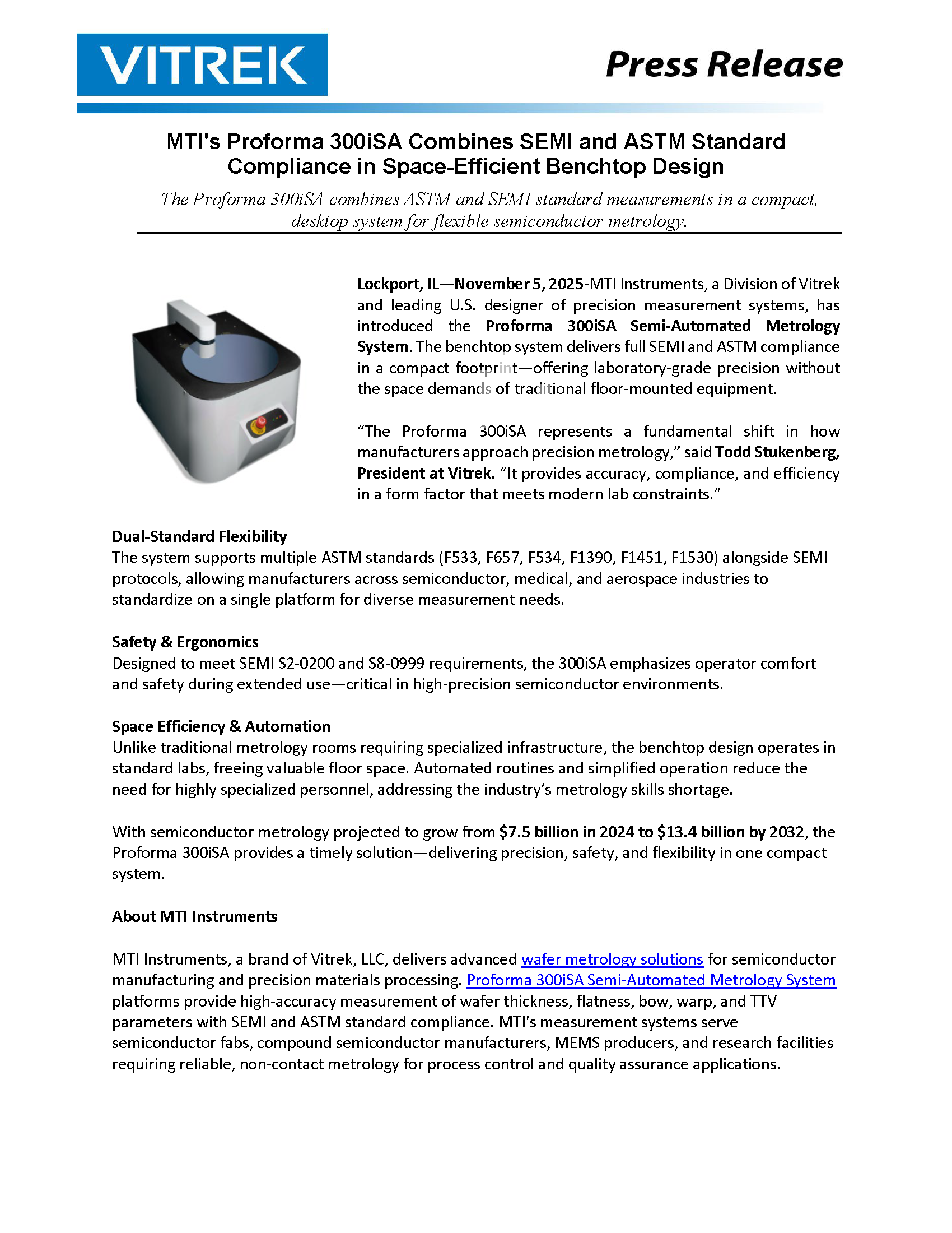
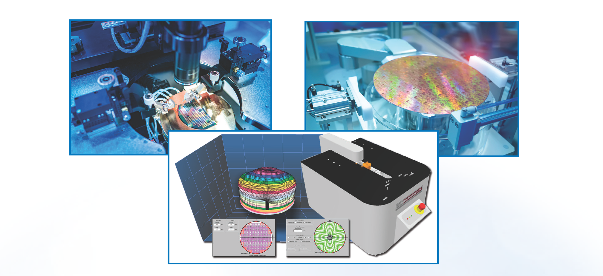
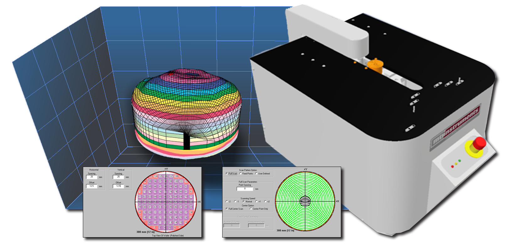
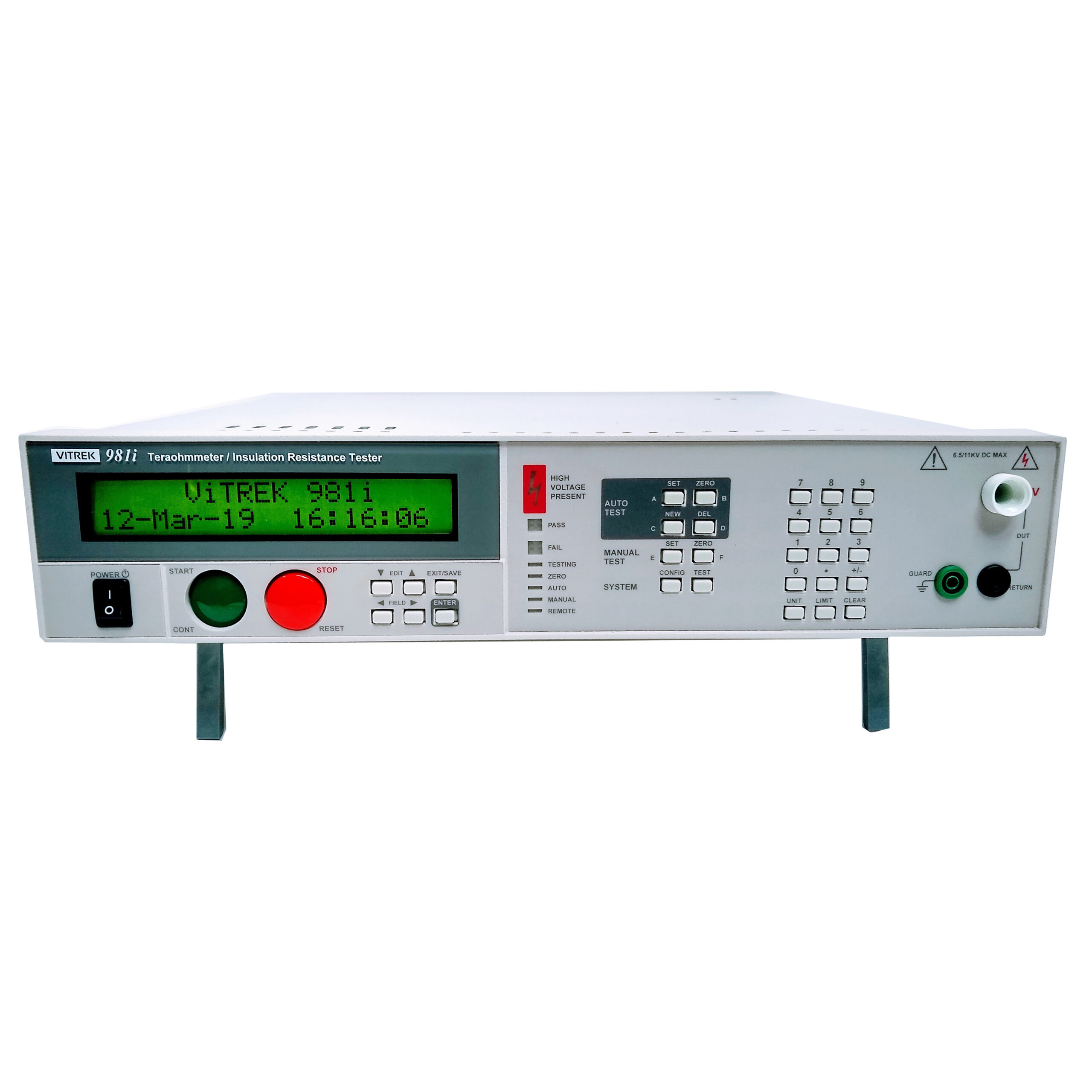
Vitrek’s MTI Proforma 300i and Proforma 300iSA is a non-contact metrology solution for wafer measurement that uses proprietary capacitance-based technology to perform non-contact wafer measurements. The Proforma 300i is a manual system suited to point-based thickness measurements. Operators can use defined measurement locations to verify thickness and evaluate total thickness variation without physically contacting the wafer surface.
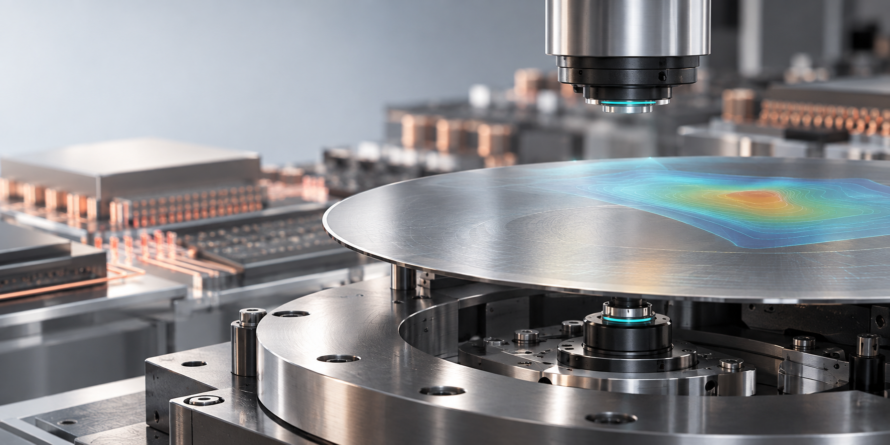
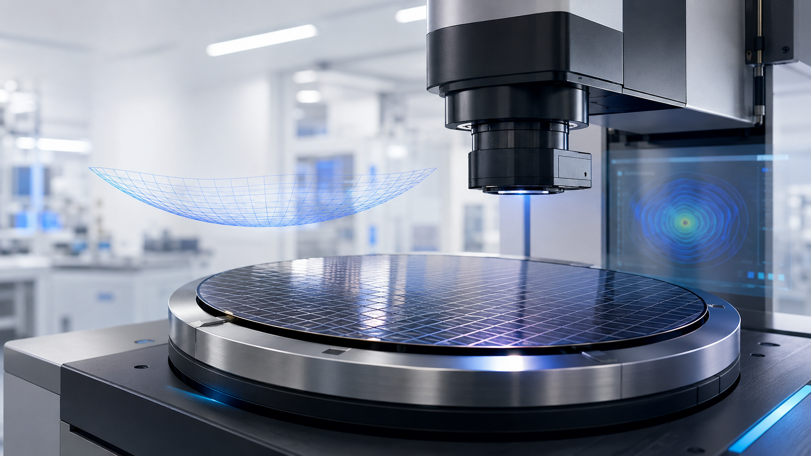
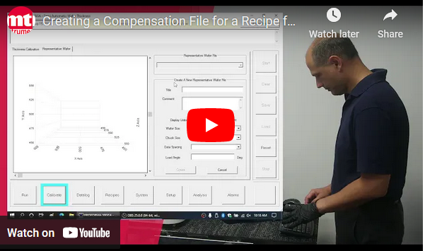
The Proforma 300iSA is a semi-automated system that expands the measurement process to programmable wafer scanning. It can collect data across multiple locations to characterize thickness, total thickness variation, bow, warp, site flatness and global flatness.
The systems provide thickness accuracy of ±0.25 μm and resolution of 0.05 μm. The Proforma 300iSA can collect as many as 1,000 measurement points per minute, depending on the measurement routine and configuration.
These capabilities allow process engineers to move beyond a single center-point reading. A mapped data set can help distinguish a uniform thickness shift from localized non-uniformity, edge effects or wafershape changes.
The appropriate system configuration, fixture and qualified measurement range must be confirmed for the wafer material, diameter, thickness and process stage. This is particularly important for extremely thin wafers, bonded structures and wafers mounted to carriers or tape.
Example Process: Preparing Wafers for AI Packaging
Consider a manufacturer preparing semiconductor wafers for an AI accelerator package that combines logic and stacked memory.
The wafer enters backside processing at its original substrate thickness and progresses through coarse grinding, fine grinding and polishing. The manufacturer establishes measurement checkpoints after each operation.
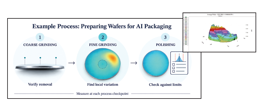 Following coarse grinding, operators verify that the process removed the intended amount of material without creating excessive thickness variation. After fine grinding, a multi-point or mapped measurement is used to evaluate uniformity and identify regional differences. A final qualified inspection is performed after polishing before the wafer advances to bonding or assembly.
If the measurements reveal that one region is thinning more quickly than another, engineers can investigate the grinding recipe, wafer support, equipment condition or alignment before processing the next lot. If wafer shape changes unexpectedly, the team can evaluate whether the condition is related to handling, residual stress, films or the thinning process itself.
The result is a controlled progression toward the required package geometry instead of relying solely on final inspection.
Supporting HBM and Chiplet Manufacturing
HBM and chiplet architecture depend on the integration of multiple components within tightly controlled physical dimensions. Thickness and geometry data can support several associated manufacturing objectives:
- Maintaining package-height targets
- Improving consistency before bonding and stacking
- Identifying non-uniform material removal
- Monitoring wafer shape as substrate stiffness decreases
- Supporting process-development and equipment-qualification work
- Preventing unsuitable wafers from reaching expensive assembly steps
- Creating traceable data for statistical process control
The measurement strategy should reflect the process decision being made. A manual point check may be appropriate for incoming inspection, process development or lower-volume work. Automated mapping provides greater insight when engineers must evaluate full-wafer uniformity, shape or repeatable production recipes.
Conclusion
AI accelerators, high-bandwidth memory and chiplet-based devices have moved advanced packaging to the center of semiconductor performance. As more components are stacked and integrated, the dimensional margin available to each wafer and die becomes increasingly limited.