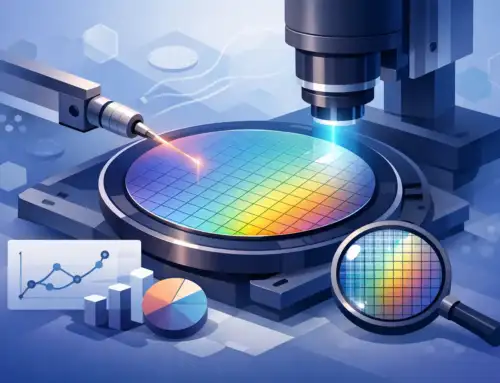
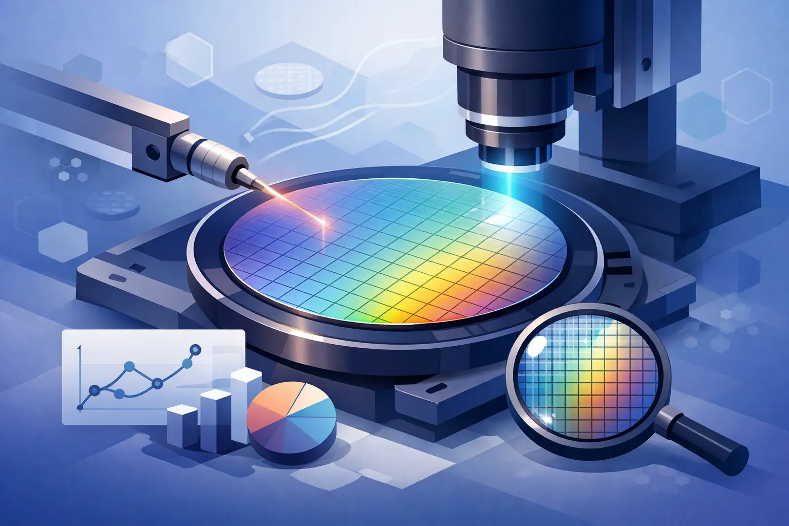
A few microns of thickness variation can move a wafer from acceptable to scrap, especially when downstream lithography, grinding, bonding, or packaging steps have little tolerance left to absorb error. That is why semiconductor wafer thickness measurement is not a routine dimensional check. It is a control point that influences yield, tool setup, process stability, and confidence in every subsequent operation.
In high-volume fabs and advanced packaging lines, thickness data has to do more than confirm a nominal value. It needs to be repeatable across lots, traceable for quality systems, and fast enough to support production decisions. In R&D and pilot environments, the same measurement often needs higher flexibility because engineers are working with varied materials, diameters, and process conditions. The right method depends on the wafer, the stage of manufacturing, and the level of uncertainty the application can tolerate.
Why semiconductor wafer thickness measurement matters
Wafer thickness affects mechanical behavior, thermal performance, and process compatibility. A substrate that is slightly out of range may still look acceptable during handling, yet create alignment issues in lithography, breakage risk in back-end steps, or inconsistent performance in bonded assemblies. Thin wafers are especially unforgiving because small force errors, vacuum chuck distortion, or local bow can change the reading enough to affect process decisions.
This is also why thickness cannot be considered in isolation. For many applications, the measured value has to be interpreted alongside total thickness variation, bow, warp, surface quality, and edge condition. If a process engineer sees a drift in final wafer thickness after grinding, the next question is usually whether the issue is uniform removal, fixture setup, chucking effects, or metrology setup. A single number is rarely enough.
In regulated and performance-critical manufacturing, measurement traceability is equally important. If incoming wafer lots are qualified to one tolerance and outgoing product is validated to another, the thickness measurement system becomes part of the quality record. That raises the bar for calibration discipline, repeatability studies, and operator consistency.
The main methods used for wafer thickness measurement
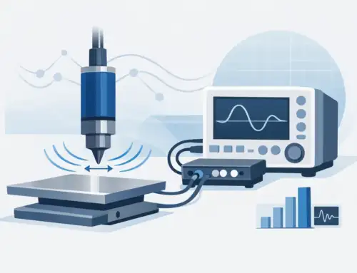
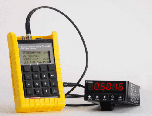
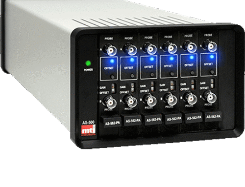
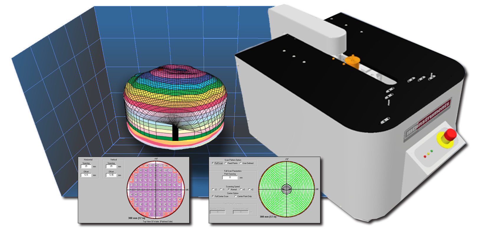
Several approaches are used in semiconductor environments, but non-contact displacement metrology is often preferred because it reduces risk to delicate surfaces and supports automation. The most common setup measures the distance to the top and bottom wafer surfaces and calculates thickness from the differential. Capacitive, confocal, chromatic, optical, and laser-based methods may all be considered, depending on material properties and required resolution.
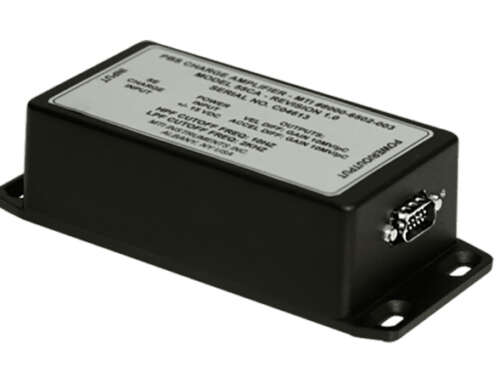
Capacitive sensing is widely used where very high resolution and stable non-contact measurement are required. It performs well when the target material and setup are compatible with the sensing principle, and it is especially strong in precision displacement applications. For conductive or appropriately configured targets, capacitive systems can deliver the repeatability needed for thin wafer measurement and process control.
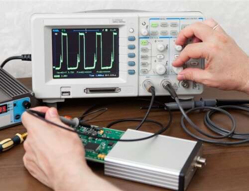
Optical methods offer flexibility when materials vary or when non-contact access is constrained. They can be effective, but surface reflectivity, transparency, roughness, and multilayer structures all influence performance. A polished silicon wafer behaves differently from a compound semiconductor substrate or a thinned wafer with films and backside treatment. The method that works well in one process step may require adjustment in another.
Mechanical contact measurement is still used in some lab or offline settings, but it introduces trade-offs. Contact force can distort thin wafers, damage sensitive surfaces, or reduce repeatability when operator technique varies. For high-value substrates and automated production, that is usually not the preferred path.
What makes a thickness measurement reliable
A reliable wafer thickness result starts with fixture control. If the wafer is not supported consistently, local deflection can appear as thickness variation. Vacuum handling helps with positioning, but excessive or uneven chuck force can alter the measurement, particularly on thinned wafers. The fixturing approach has to match wafer thickness, diameter, and stiffness.
Sensor alignment is another critical factor. In dual-sided measurement systems, the top and bottom sensors must be aligned so they are effectively measuring the same point. Any offset can mix true thickness with local bow, warp, or surface profile. That is manageable if the system is designed for it and the application accounts for it, but it cannot be ignored.
Environmental control matters more than some users expect. Temperature drift changes both the wafer and the metrology hardware. Vibration, air turbulence, and contamination can introduce noise that is small in absolute terms yet significant relative to a sub-micron tolerance. For engineering teams trying to reduce uncertainty, good metrology practice often delivers more value than a nominally higher-spec sensor used in a poor setup.
Calibration strategy also deserves attention. A system should be verified against traceable standards appropriate to the expected thickness range and accuracy requirement. The calibration interval depends on usage, environment, and quality requirements, but in production environments the larger concern is usually not just whether the sensor was calibrated, but whether the entire measurement process was validated under real operating conditions.
Common error sources in semiconductor wafer thickness measurement
The most common mistake is assuming that sensor resolution and measurement accuracy are the same thing. A system may display very fine increments while still being vulnerable to setup error, thermal drift, target effects, or stage motion. Engineers evaluating systems should look at total measurement uncertainty under application conditions, not just best-case sensor specifications.
Material behavior is another source of variation. Transparent or semi-transparent wafers can challenge optical methods because multiple reflections may be detected. Highly reflective surfaces can saturate certain optical systems, while rough or processed surfaces can scatter light unpredictably. Capacitive approaches bring their own application constraints related to target properties and grounding conditions.
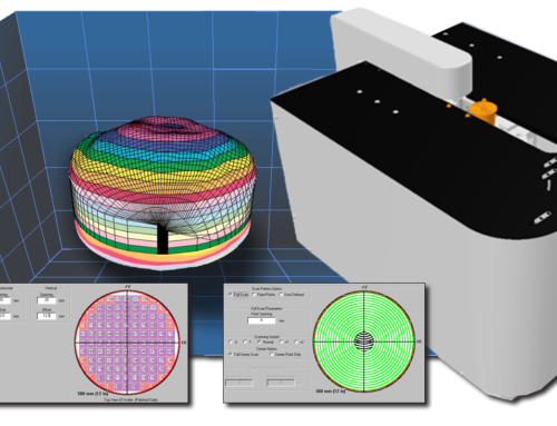
Then there is wafer geometry. Bow, warp, notch orientation, edge roll-off, and local thickness variation all change what the instrument sees. If the goal is a center-point thickness check, the system can be optimized for that. If the goal is full-wafer mapping, the motion system, sensor bandwidth, and data handling become just as important as the sensing principle.
Operator workflow can also create error. A cleanroom-compatible measurement system that loads predictably, aligns consistently, and automates recipe selection often produces better real-world results than a more complex instrument that depends on manual setup. Precision hardware matters, but repeatable use matters just as much.
Choosing a system for production, R&D, or incoming inspection
The right system depends on what decision the data is meant to support. In incoming inspection, the priority may be fast verification against supplier specifications with documented traceability. In process development, engineers may need high-resolution data across different wafer materials and process states. In production, throughput, automation, and repeatability usually outrank maximum flexibility.
For backgrinding and thinning processes, focus on non-contact measurement stability, wafer handling, and the ability to characterize thin substrates without introducing stress. For epitaxy or polished wafer inspection, surface condition and material response will influence sensor selection. For advanced packaging, where die, carrier, and bonded structures may all be involved, the measurement problem can extend beyond a single bare wafer.
System integration is often overlooked during procurement. If thickness data needs to feed SPC software, MES infrastructure, or a custom process control environment, the metrology platform should support that workflow from the start. The same applies to maintenance and calibration support. An accurate instrument with poor serviceability can become a bottleneck in a regulated manufacturing line.
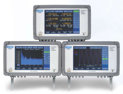
This is where application-specific metrology platforms from established instrumentation suppliers tend to separate themselves from generic measurement tools. Companies such as Vitrek, through its broader precision metrology portfolio, address these environments by focusing on repeatable measurement architecture, supportability, and the practical realities of industrial deployment.
Using thickness data effectively
Thickness measurement creates the most value when it is treated as process intelligence, not just inspection output. Trend data can reveal grinding wheel wear, fixture drift, upstream material changes, or equipment instability before parts move out of tolerance. Mapping can distinguish localized tool effects from wafer-to-wafer variation. Correlating thickness with bow and total thickness variation can shorten root-cause analysis substantially.
It also helps to define what action a result should trigger. If a wafer is out of spec by a small margin, is that a hold, a rework candidate, or a sign that process centering needs adjustment? Metrology is most useful when the limits, sampling plan, and response plan are all defined before problems appear.
For engineers and quality teams, the practical question is not whether wafer thickness can be measured precisely. It can. The real question is whether the selected method, fixture, calibration approach, and data workflow are aligned with the process risk. When they are, semiconductor wafer thickness measurement becomes a dependable control tool instead of another variable to manage.
The closer tolerances get, the less room there is for assumptions. Good thickness metrology earns its place by reducing uncertainty where it matters most – on the line, in the lab, and in the decisions built on the data.


