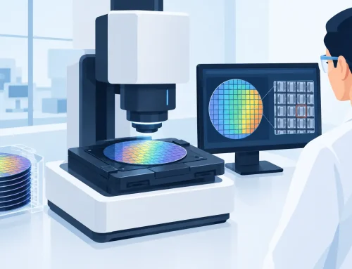
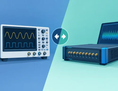
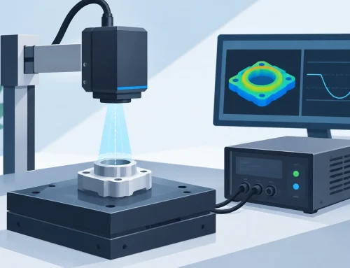
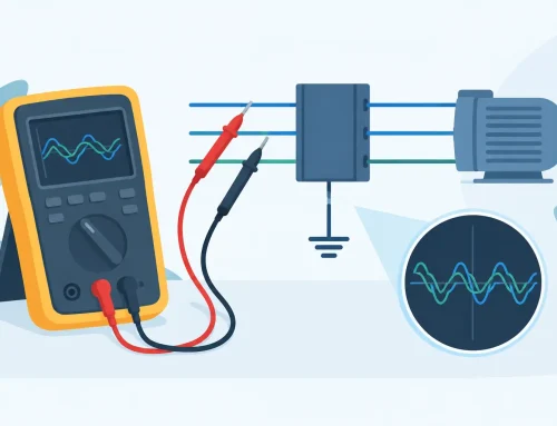
A wafer can meet a nominal thickness specification and still create downstream yield risk. Local thickness variation, bow, warp, edge effects, and surface geometry can affect lithography focus, deposition uniformity, bonding, handling, and device performance. A disciplined wafer metrology process guide helps engineering and quality teams turn those physical conditions into repeatable, decision-ready data rather than isolated measurements.
The objective is not simply to collect more points. It is to define the wafer characteristic that matters, measure it with known uncertainty, and connect the result to an acceptance limit or process action. That approach is especially important when measurements support supplier qualification, incoming inspection, process development, equipment matching, or statistical process control.
Start With the Measurement Decision
Every metrology plan should begin with the question the data must answer. A process engineer evaluating grinding may need total thickness variation and local site flatness. A lithography team may be more concerned with bow, warp, and focal-plane behavior. A quality team receiving polished wafers may need confirmation that material meets a drawing, purchase specification, or applicable SEMI-defined method.
This distinction determines the measurement method, sampling density, reference scheme, and reporting format. It also prevents a common failure: using a single center-point thickness value to represent a wafer whose edge region or local topology is the actual source of concern.
Define the following before selecting a system or writing a measurement routine:
- The measurand, including thickness, total thickness variation, bow, warp, site flatness, nanotopography, or another specified parameter
- The wafer material, diameter, thickness range, surface finish, transparency, backside condition, and presence of films or patterns
- The applicable specification, including edge exclusion, sites, sampling grid, reference plane, and reporting units
- The required measurement uncertainty and decision rule for pass/fail disposition
- The intended use of the data, such as process adjustment, release inspection, supplier control, or engineering characterization
The definition of the measurand deserves particular attention. Thickness is generally the distance between frontside and backside surfaces at a specified location. Total thickness variation is the range between maximum and minimum thickness across the defined measurement area. Bow and warp are shape parameters, but their reported values depend on the selected reference methodology and support condition. Values from different tools or methods should not be treated as interchangeable unless the definitions, setup, and analysis rules align.
Build the Wafer Metrology Process Guide Around the Surface
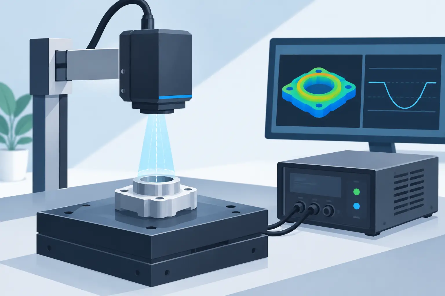
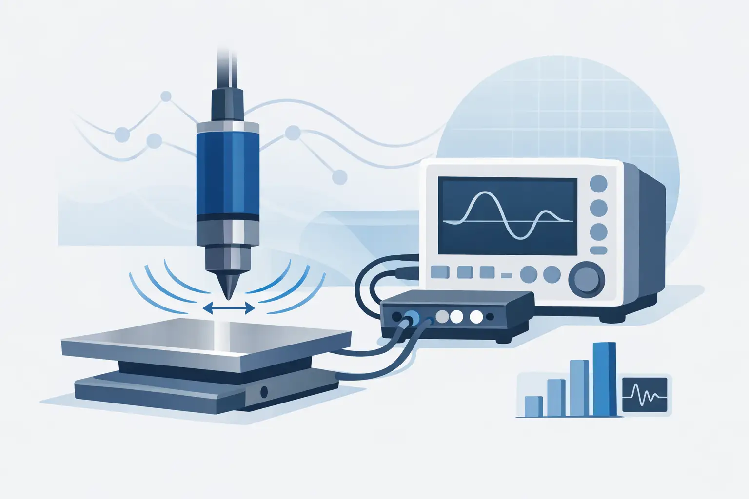
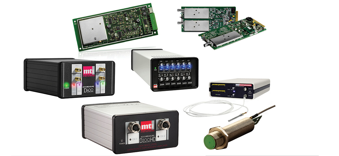
The wafer itself drives much of the system design. Optical methods can provide fast, non-contact measurement, but material transparency, film stack properties, reflectivity, surface roughness, and patterned features may influence signal quality. Capacitive techniques can offer high sensitivity for conductive targets, while their performance depends on gap control, alignment, and the electrical properties of the measured surface.
For geometry measurements requiring front-to-back information, the fixture and handling method are part of the measurement system. A wafer supported differently can exhibit different apparent shape because gravity, vacuum chucking, edge support, and mechanical stress influence the observed profile. The process documentation should state whether the wafer is measured free-standing, on a chuck, or with a specified support geometry.
Environmental control also matters. Temperature changes affect both wafer dimensions and instrument structure. Vibration, airborne contamination, electrostatic attraction, and thermal gradients can degrade repeatability, particularly in thin wafers or submicron applications. A capable sensor cannot compensate for a poorly controlled measurement cell.
For production use, document the operating envelope: temperature range, warm-up time, vibration limits, cleaning procedures, wafer orientation, handling requirements, and acceptable recovery actions after an interrupted measurement. This turns experienced operator practice into a controlled process.
Establish a Repeatable Coordinate System
A measurement map has little value if the coordinate system shifts from wafer to wafer. Use the notch, flat, or another approved datum to establish orientation. Define the center determination method, measurement radius, edge exclusion, and angular convention. If site measurements are used, specify site size and position rather than relying on visual placement.
Edge exclusion is not an administrative detail. The outer region often has different polishing behavior, bevel geometry, film coverage, and handling risk. Including or excluding it can materially change a reported thickness variation or flatness result. The selected boundary must match the product requirement and remain fixed across lots, tools, and locations.
Select Sampling Density That Can See the Failure Mode
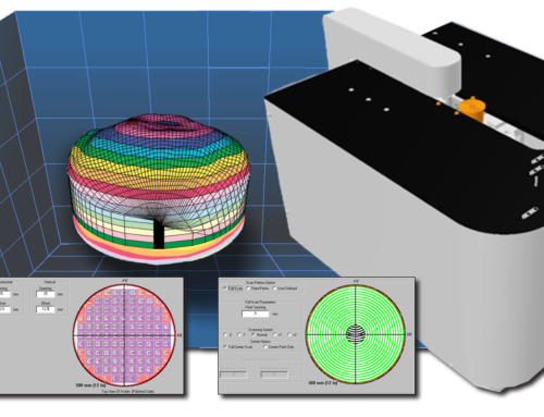
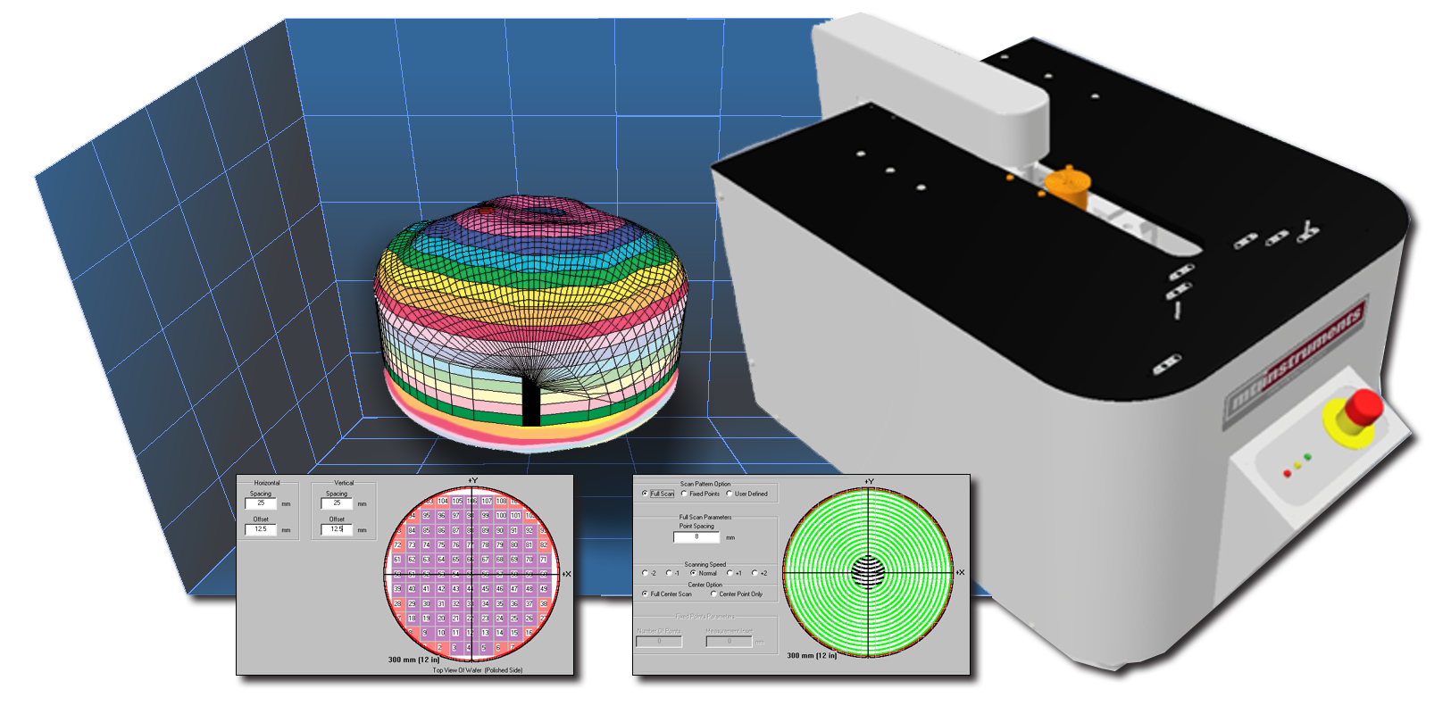
A sparse map is faster, but it can miss local variation. A dense map improves spatial visibility, but it increases cycle time, data volume, and sensitivity to measurement noise. The appropriate density depends on the spatial scale of the defect or process signature being controlled.
For example, a broad radial thickness trend may be visible with a moderate grid. Local polishing artifacts, chuck-related signatures, or handling damage may require more closely spaced samples or area-based scanning. If the wafer will move into a process with tight local planarity requirements, a small number of widely separated points may be inadequate even when the average result looks acceptable.
A practical approach is to use two measurement tiers. Use a faster, defined sampling plan for routine production screening, then trigger higher-density characterization when control limits are exceeded, a new material lot is introduced, or a process change occurs. The trigger criteria should be documented in the control plan rather than left to operator judgment.
Verify the Measurement System Before Trusting Trends
Metrology data is only as useful as the measurement system analysis behind it. Calibration traceability, repeatability, reproducibility, bias, resolution, and stability should be evaluated for the actual wafer application, not only from a generic instrument specification.
Calibration standards should be appropriate for the measurement range and maintained on a documented schedule. For thickness work, confirm that the standard and method exercise the relevant measurement path. For shape measurements, verify the system response using artifacts or reference wafers that represent the geometry range of interest. A calibration result alone does not establish that the installed process, fixture, environmental conditions, and software recipe are suitable.
A repeatability and reproducibility study should include normal production variation. Use representative wafer sizes, materials, surface conditions, and operators where applicable. If a fully automated system is used, repeatability may dominate; if manual loading, alignment, or recipe selection is involved, reproducibility can be the larger risk.
Pay close attention to uncertainty near a specification limit. When the expanded uncertainty is a meaningful fraction of the tolerance, a simple pass/fail declaration may create false accepts or false rejects. Establish a decision rule that defines how uncertainty is handled, including any guard band used for release decisions. This is particularly relevant for customer specifications, regulated applications, and supplier disputes.
Turn Raw Data Into Process Control
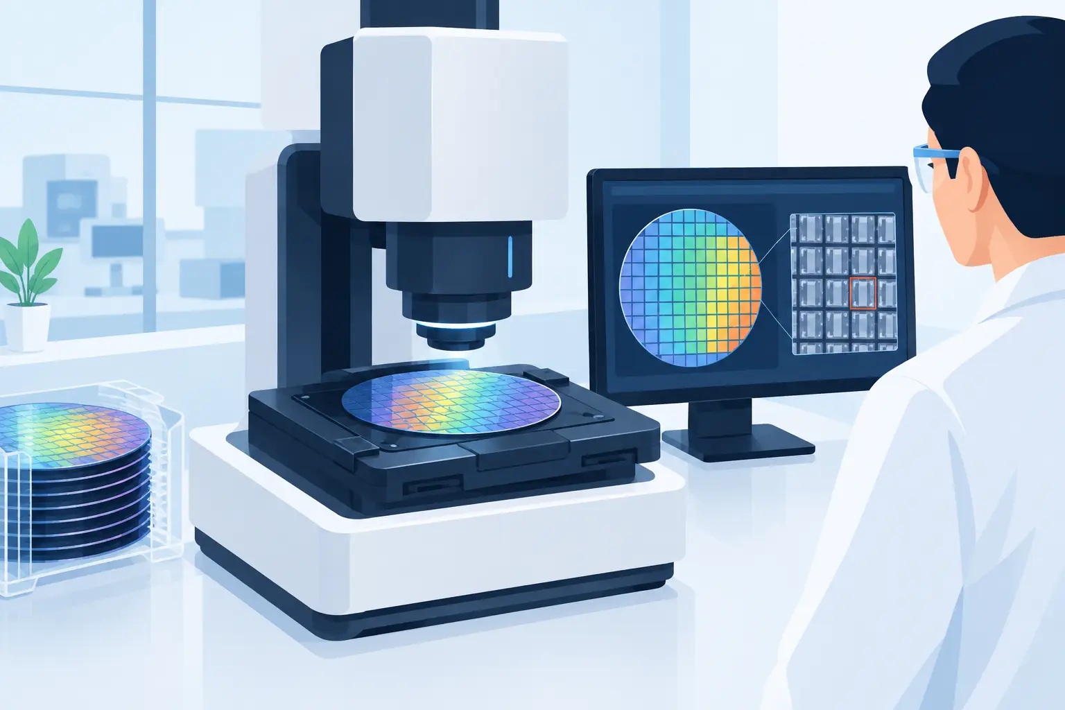
A wafer map should lead to an action. Reporting only minimum, maximum, and average values can conceal the shape of a developing process problem. Retain spatial plots and trend the parameters that are tied to the process mechanism. A rising center-to-edge thickness difference, for example, points to a different investigation than random local excursions.
Control charts are effective when they distinguish normal process variation from special-cause changes. Establish baseline behavior using stable production data, then monitor appropriate statistics by product family, wafer size, material type, and process route. Combining unlike products into one trend can produce limits that are too broad to be useful.
When a limit is exceeded, preserve the contextual data: instrument identification, calibration status, recipe revision, operator or automation log, environmental conditions, lot history, and any recent maintenance. This record shortens root-cause analysis and supports traceability when data is reviewed months later.
Common Sources of Misleading Results
Many apparent wafer failures originate in the measurement process. Particles beneath a wafer on a chuck can create localized distortion. Incorrect notch alignment can shift site locations. A changed edge-exclusion setting can alter a calculated total thickness variation without any actual process change. Mixing results from tools with different reference algorithms can create a trend that exists only in the reporting method.
Another frequent issue is treating sensor resolution as total system accuracy. Resolution describes the smallest displayed increment under defined conditions. Accuracy and uncertainty also include calibration, linearity, fixture effects, alignment, environmental influences, surface interaction, and analysis method. Engineering decisions should be based on the full measurement capability.
The most effective wafer metrology programs make uncertainty visible, standardize the setup, and preserve enough context to explain each result. When the data is trusted, it becomes more than an inspection record: it becomes an early indicator of process health and a defensible foundation for semiconductor manufacturing decisions.