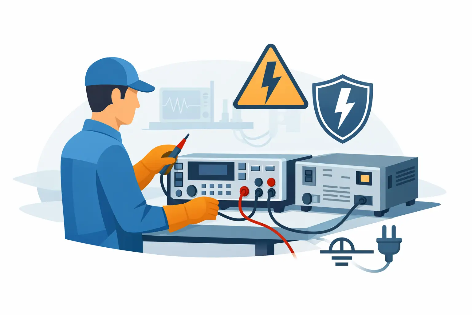
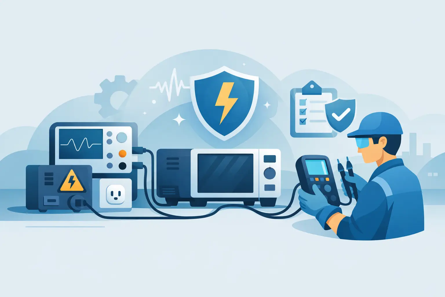
A hipot failure at 1,500 V does not always mean the product is unsafe. Just as often, it means the test limit was selected without enough attention to insulation system design, applicable standards, altitude, leakage behavior, or the difference between production screening and design validation. That is why dielectric withstand test limits deserve more rigor than a simple rule-of-thumb multiplier.
For engineers and compliance teams, the central issue is straightforward: a dielectric withstand test must apply enough stress to reveal insulation weaknesses without overstressing a conforming product. The difficulty is that those limits are never universal. They depend on the product category, insulation class, working voltage, pollution degree, overvoltage category, materials, construction, and the specific standard that governs the equipment.
What dielectric withstand test limits actually define
Dielectric withstand test limits define the maximum test voltage, test duration, and sometimes current trip conditions used to verify that insulation can tolerate an electrical stress above normal operating conditions. In practical terms, the limit is not just a voltage number. It is a test boundary that combines applied potential, ramp profile, dwell time, and pass-fail criteria.
That distinction matters because two tests with the same nominal voltage can produce different outcomes. A slow ramp may allow capacitive charging current to settle before the measurement window. A short dwell may reduce the chance of detecting marginal insulation. AC and DC methods can also stress the device differently, especially where distributed capacitance or nonlinear leakage paths are involved.
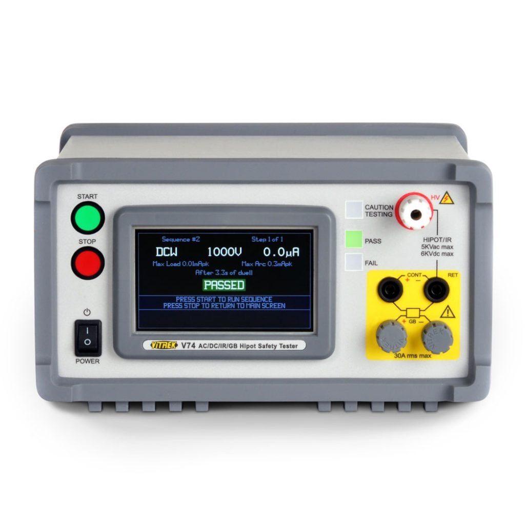
In regulated manufacturing, dielectric withstand test limits are typically defined by product safety standards rather than by tester capability. The instrument should be selected to execute the required method accurately and repeatably, not to determine the method on its own.
How dielectric withstand test limits are set
In most applications, the first source is the governing standard. For medical, industrial, consumer, laboratory, or EV-related equipment, the relevant safety framework usually specifies insulation coordination requirements and the associated verification tests. Those requirements often tie the withstand level to rated mains voltage, insulation type, and intended use environment.
From there, engineering judgment still matters. A standard may permit multiple test approaches, different voltage formulas, or reduced production test times after type testing. It may also distinguish between basic insulation, supplementary insulation, reinforced insulation, and protective impedance. Each case can lead to a different limit.
The product itself can narrow the acceptable range further. Assemblies with high stray capacitance, EMI filters, surge suppressors, long cable runs, or moisture-sensitive materials may need careful interpretation of test current limits and ramp rates. The right dielectric withstand test limit is therefore the point where compliance intent, product physics, and test practicality stay aligned.
Working voltage is only the starting point
Many teams begin with rated operating voltage, then apply a multiplier. That is common practice, but it is incomplete. Working voltage influences insulation stress over time, yet withstand testing is also shaped by transient expectations, spacing requirements, and the insulation system’s role in protecting users and equipment.
For example, reinforced insulation is expected to tolerate more severe stress than functional insulation because the consequence of failure is different. In the same way, equipment intended for controlled laboratory space may be evaluated differently than equipment installed in harsher industrial environments. The numeric test limit reflects those distinctions.
Environment changes the limit
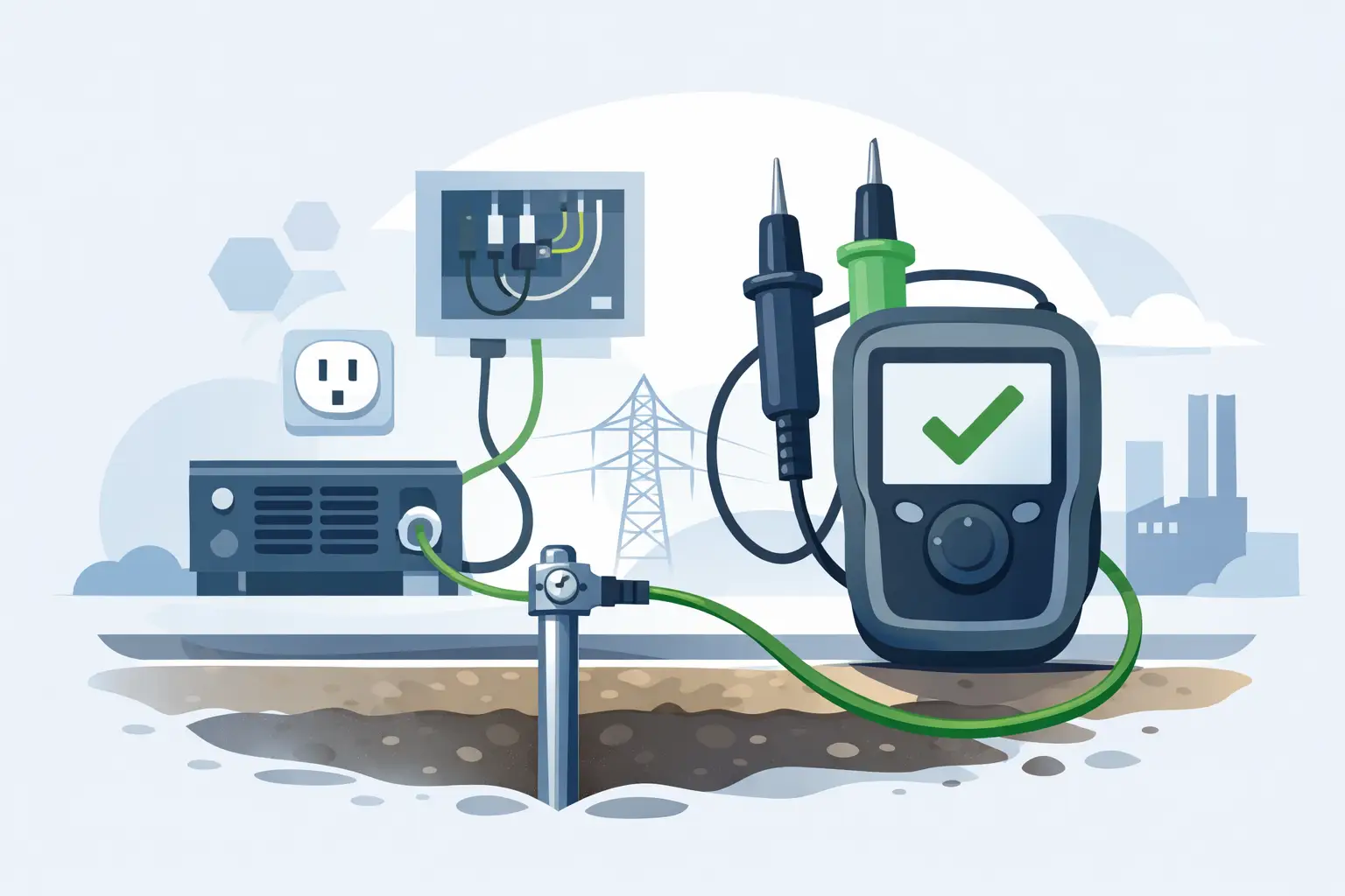
Altitude, humidity, contamination, and installation category can materially affect dielectric behavior. At higher altitudes, reduced air density lowers breakdown strength, which can force derating or adjusted test interpretation. Pollution degree and material group influence creepage and clearance design, which in turn affects whether the selected withstand level is realistic for the finished assembly.
This is where test planning often improves product outcomes. If a product is likely to be used above a standard reference altitude, the design team should account for that before production test limits are finalized. Otherwise, a unit may pass in one environment and become marginal in another.
Why passing at a higher voltage is not always better
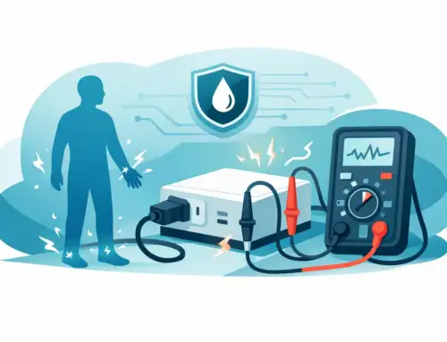
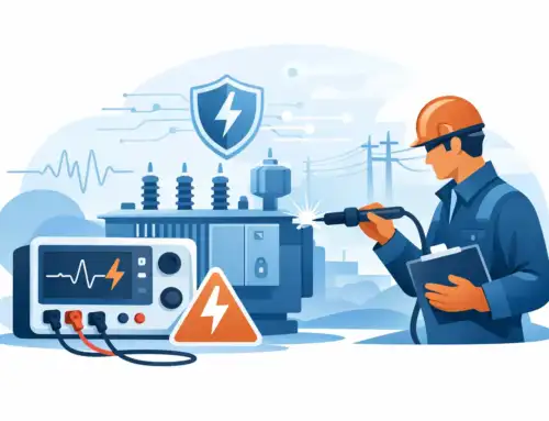
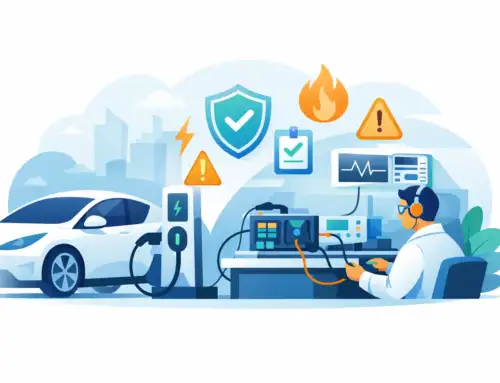
A common mistake is assuming that more test voltage means more safety margin. In reality, excessive hipot stress can damage insulation that would perform reliably in normal service. Thin dielectrics, wound components, optocouplers, relays, and tightly packed PCB assemblies can all be affected if the test level exceeds what the applicable standard or component construction supports.
This is especially relevant in high-volume production. A design validation test may justify a certain withstand level and duration under controlled conditions, but applying that same stress to every production unit can accelerate wear or create latent defects. Many standards recognize this trade-off and allow reduced duration or alternative production screening methods after initial qualification.
The engineering question is not “How high can we test?” It is “What level verifies insulation integrity without introducing unnecessary stress?” That framing leads to better limit selection and fewer false assumptions about product quality.
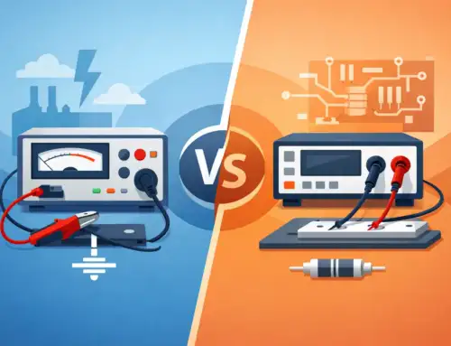
AC vs DC testing affects practical limits
AC hipot remains common because it stresses insulation in both polarities and aligns well with many traditional safety frameworks. It can also be more sensitive to certain defects. However, AC testing introduces reactive current from capacitance, which can complicate trip settings and create nuisance failures in products with filters or larger distributed capacitance.
DC hipot reduces capacitive current once the device is charged, which can make it easier to distinguish true leakage from charging effects. It is often useful where products have higher capacitance or where lower required test power is desirable. The trade-off is that equivalent stress between AC and DC is not one-to-one in every application, and the selected DC level must match the governing method.
If teams compare dielectric withstand test limits across AC and DC methods without accounting for waveform effects, they can misread both failures and margins. The test technology and the limit have to be considered together.
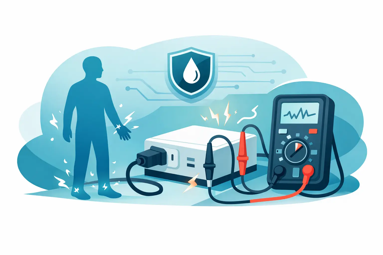
Current limits matter as much as voltage limits
A withstand test is usually judged by whether breakdown or excessive leakage occurs during the applied voltage interval. That means current trip settings are not secondary details. If the trip threshold is too low, normal charging or leakage behavior may trigger a false fail. If it is too high, the system may miss meaningful degradation or arc events.
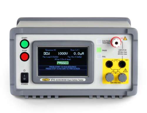
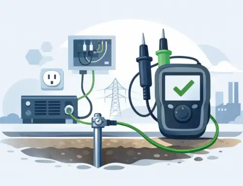
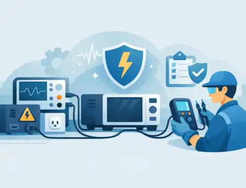
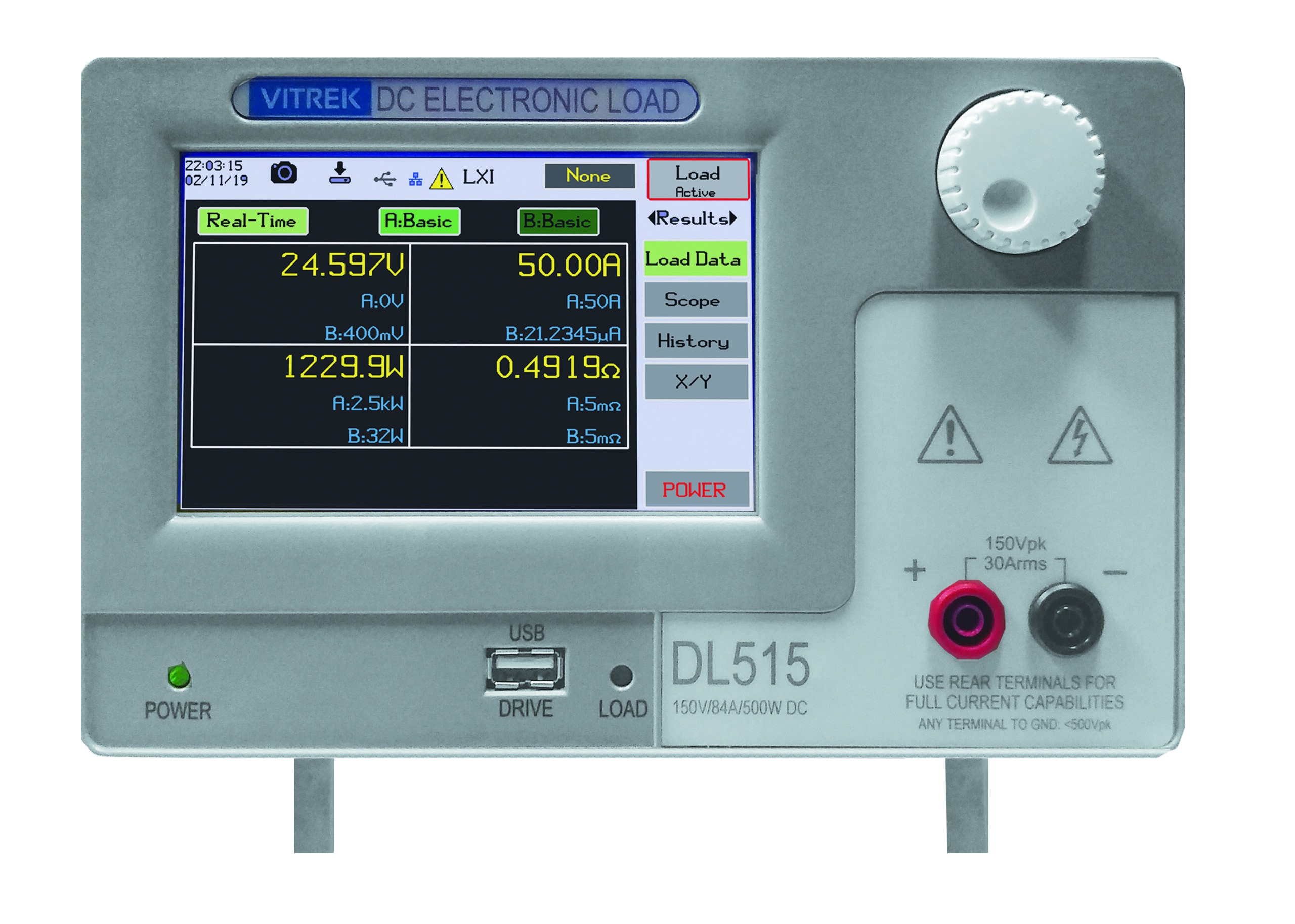
This is one reason high-quality instrumentation and repeatable fixturing matter. Test results should reflect the DUT, not variation introduced by cable placement, grounding inconsistency, poor shielding, or operator-dependent setup. In production environments, stable measurement architecture often determines whether the selected test limit is actionable.
For complex products, it is worth separating charging current, steady-state leakage, and true breakdown behavior during method development. That work usually pays for itself by reducing debug time and preventing unnecessary rejects.
Applying limits in design validation and production
Design validation should answer whether the insulation system meets the intended safety margin under worst-case conditions. Production test should confirm that each unit was built correctly and remains within the validated construction envelope. Those are related goals, but they are not identical.
During validation, teams often use more extensive stress conditions, including longer dwell times, multiple sample conditions, and environmental exposure. In production, throughput, repeatability, and component protection become more significant. A limit that is technically defensible in the lab may not be the right daily factory setting.
That is where documented rationale matters. When the standard allows flexibility, the chosen dielectric withstand test limits should be tied to design evidence, component ratings, failure mode understanding, and process capability. For organizations managing audits, certification reviews, or multi-site manufacturing, that documentation is often as important as the test result itself.
Common reasons teams get the limits wrong
The first is using a generic formula without confirming the governing product standard. The second is ignoring the difference between type test and routine production test. The third is treating all leakage current as failure current.
Another frequent issue is neglecting the total system. Connectors, harnesses, relays, transformers, coatings, and fixture interfaces can all influence the apparent withstand margin. A tester may report failure at the assembly level even when the root cause is in the interface or setup. Precision matters here, which is why many engineering teams rely on configurable safety test systems with controlled ramping, accurate leakage measurement, and traceable performance.
In high-consequence sectors such as medical, aerospace, EV, and defense electronics, conservative assumptions are understandable. But conservative does not mean arbitrary. It means the limit is technically justified, repeatable, and appropriate to the risk.
A better way to think about dielectric withstand test limits
The most effective approach is to treat the limit as part of insulation validation strategy, not as a standalone number on a traveler. Start with the applicable standard. Verify the insulation classification. Review environmental and installation assumptions. Then develop a method that matches the product’s electrical behavior, including waveform, ramp, dwell, and current criteria.
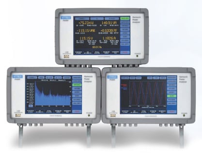
If the product includes high capacitance, sensitive components, or mixed-voltage sections, spend time on correlation before locking production settings. That is usually where avoidable false failures and overstress issues surface. For teams building test infrastructure at scale, equipment with accurate high-voltage output, repeatable measurement performance, and configurable test sequencing can make that process much more controlled. Vitrek systems are often selected for exactly that kind of standards-driven safety test environment.
Dielectric withstand testing works best when the limit reflects the product, the standard, and the physics at the same time. If those three stay aligned, the test becomes more than a pass-fail checkpoint. It becomes a reliable indicator that your insulation design is doing the job it was built to do.


