Introduction
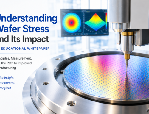
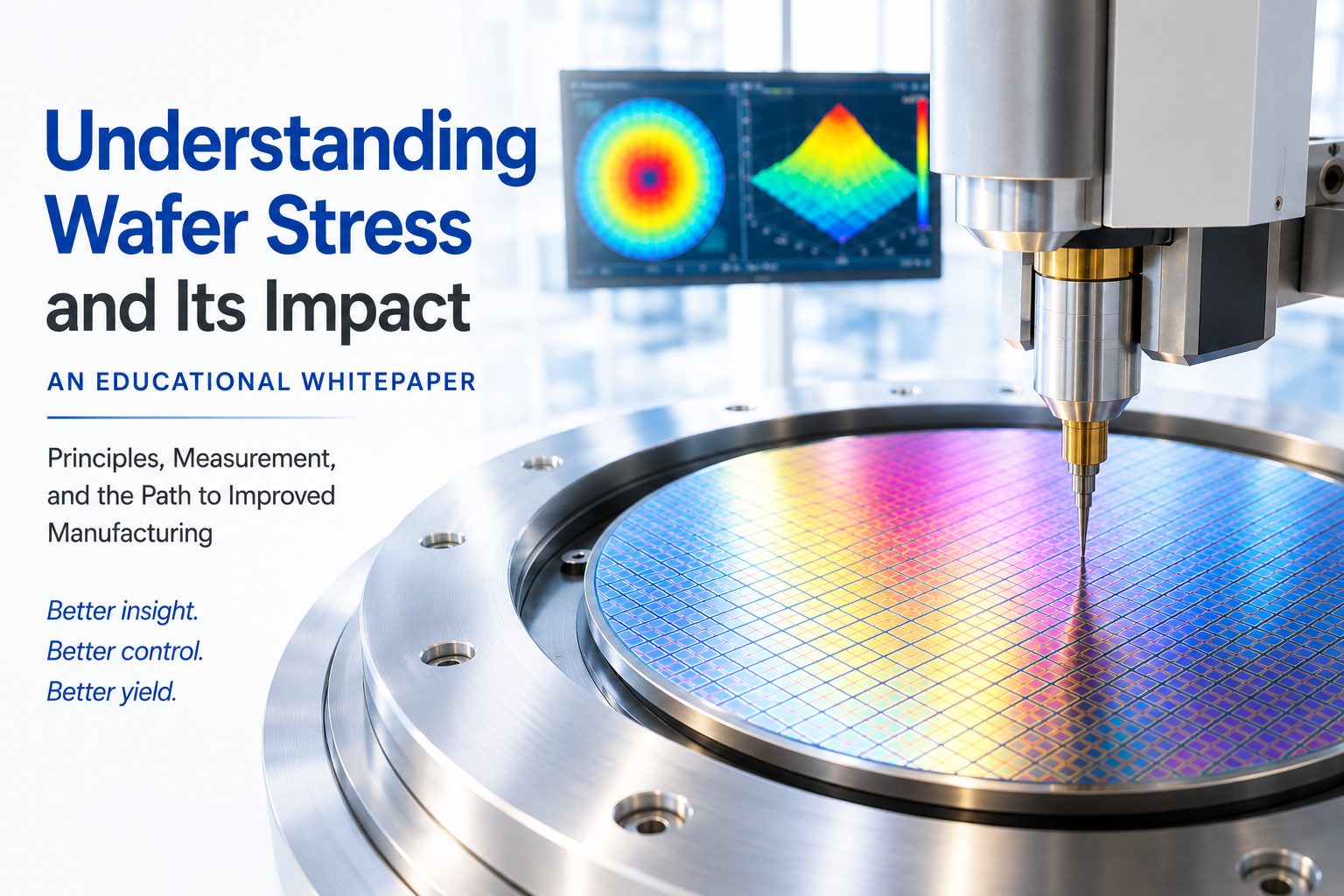
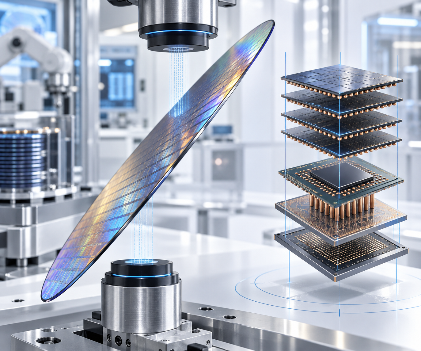
Thin films are essential to modern semiconductor devices, but every deposited, grown, bonded, or processed layer can introduce mechanical stress into the wafer. When that stress becomes excessive or inconsistent, the effects can extend well beyond the deposition step—contributing to wafer bow, cracking, delamination, overlay error, handling problems, yield loss, and downstream process instability.
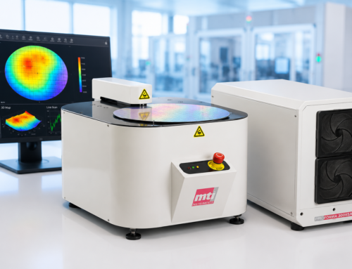
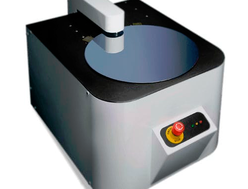
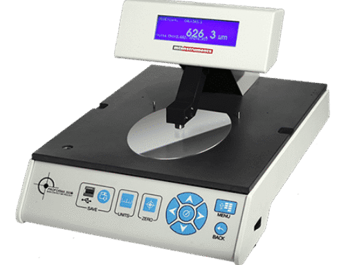
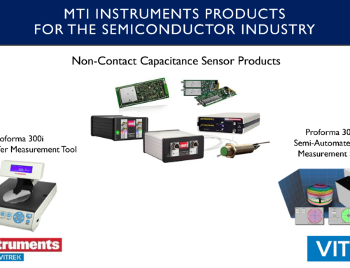
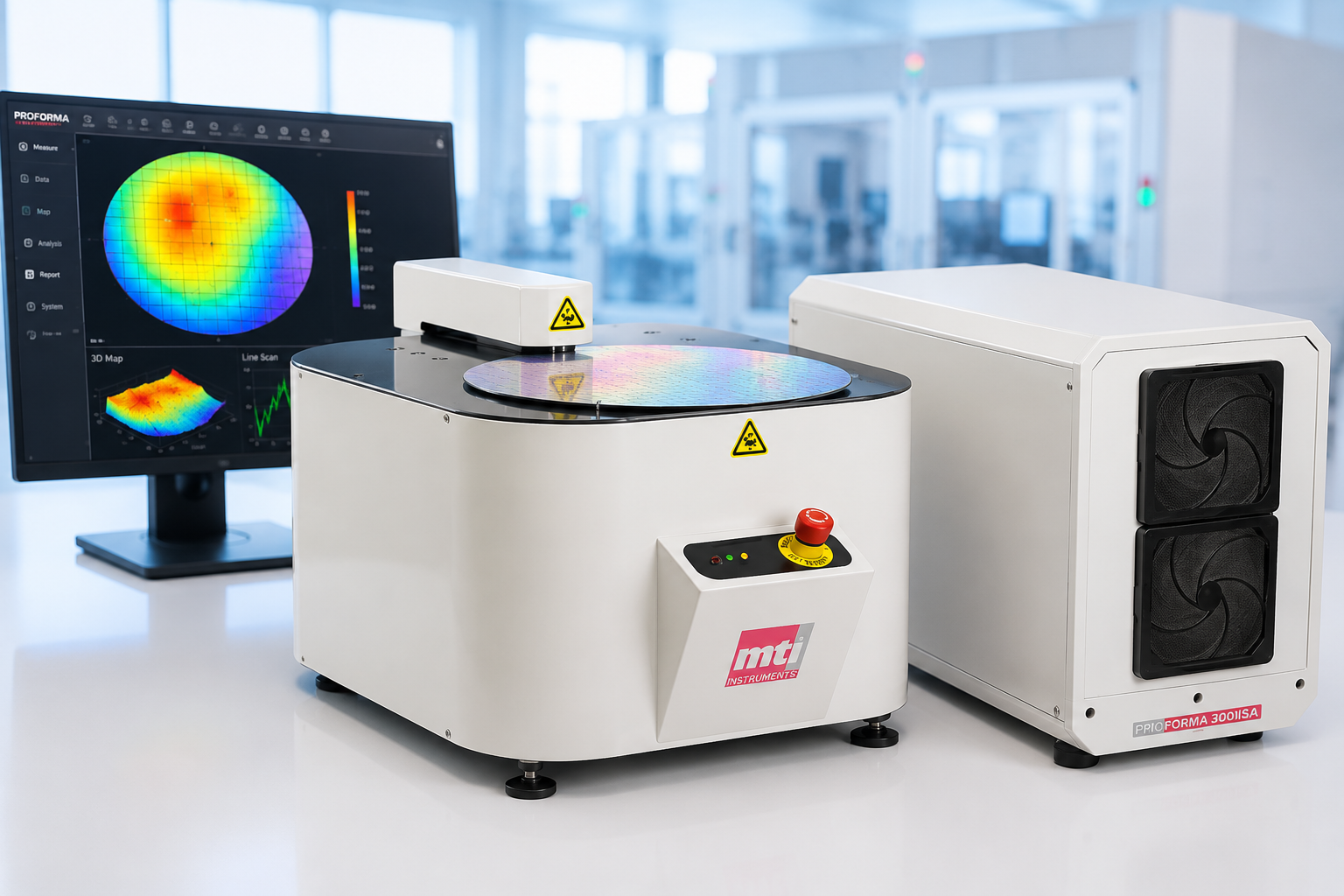
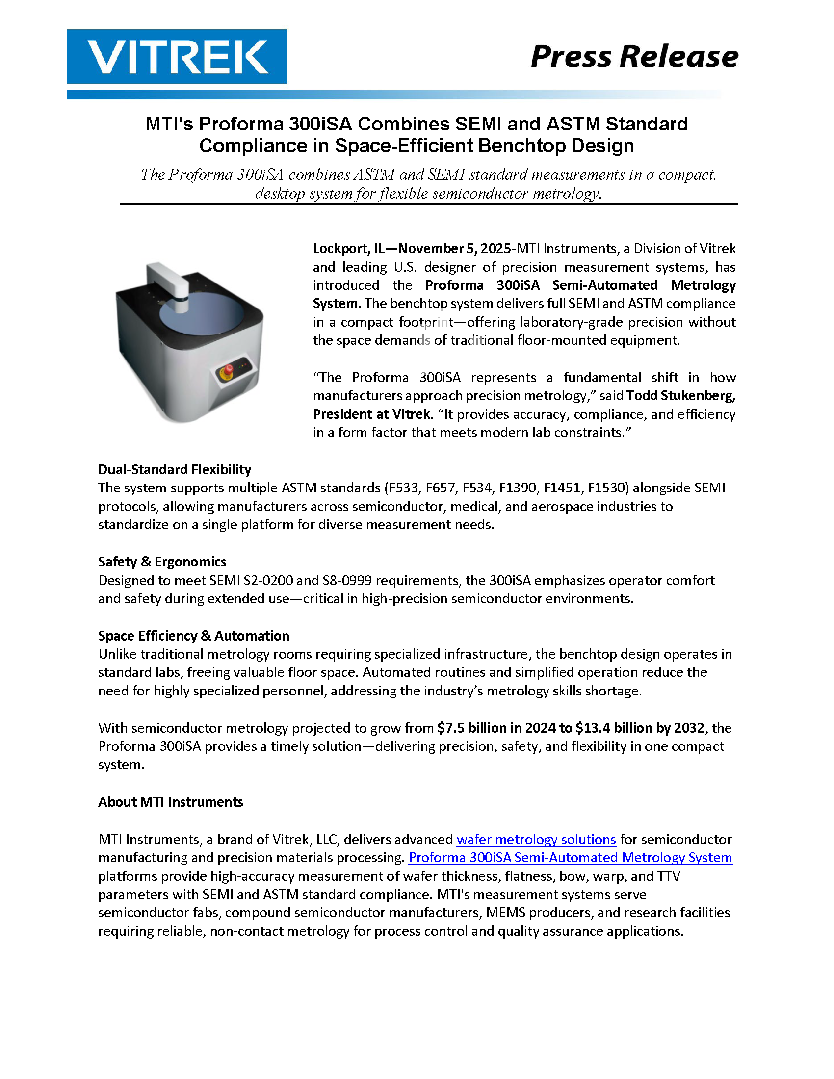
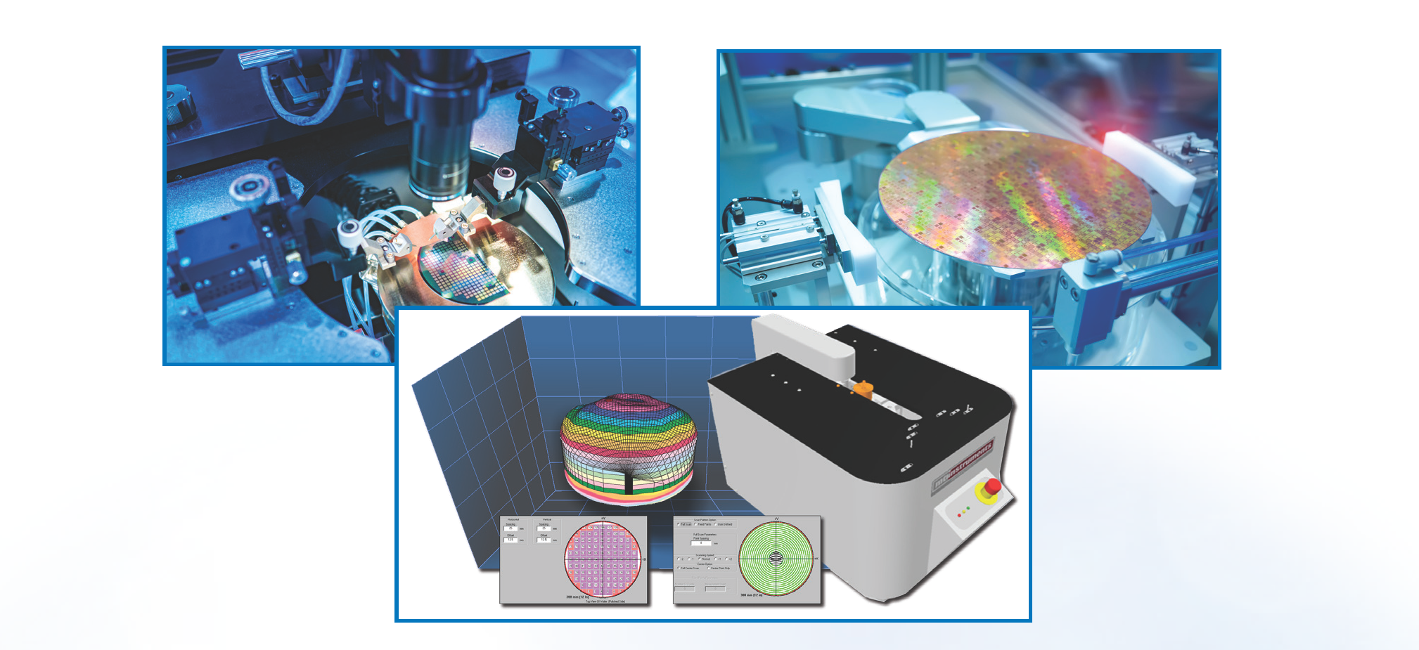
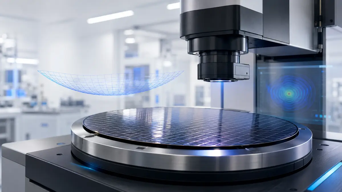
The MTI Instruments Proforma™ 300iSA semi-automated metrology system provides the full-wafer thickness and shape data needed to evaluate these risks. By measuring wafer geometry before and after a process step, engineers can quantify curvature change and use established film-stress relationships to calculate and trend stress in megapascals (MPa).
The result is a practical, non-contact approach to process characterization that helps semiconductor manufacturers, materials researchers, and packaging teams identify stress related issues early—before they become costly production problems.
Why Film Stress Matters
Film stress is the internal mechanical force present within a deposited or modified layer. It is typically expressed in megapascals (MPa) and may be:
- Tensile, where the film tends to pull the wafer surface inward
- Compressive, where the film tends to push outward
- Balanced or low stress, where the film introduces minimal wafer deformation
Neither tensile nor compressive stress is inherently unacceptable. In many device structures, a controlled level of stress is intentional and necessary. The concern is uncontrolled variation: stress that is too high, shifts from wafer to wafer, varies across the wafer, or changes unexpectedly following a process adjustment.
Even small changes in curvature can be significant. As wafers become thinner, device architectures become more complex, and process windows become
tighter, the relationship between film properties and wafer geometry becomes increasingly important.
Why Stress Measurement Matters
Stress measurement is more than a materials-characterization exercise. It is a process-control tool. Trending MPa-level stress data allows teams to
monitor deposition stability, compare recipes, qualify new materials, assess supplier consistency, and make informed corrective actions before yield is affected.
The Measurement Challenge 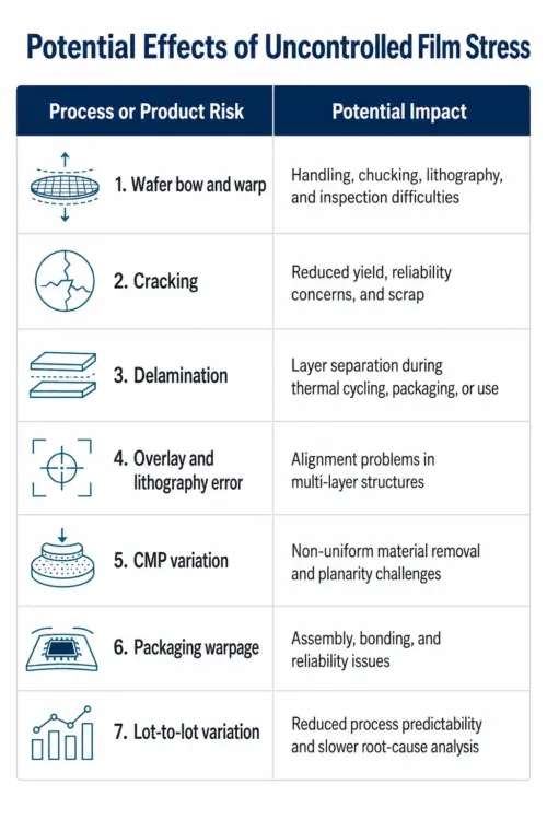
Film stress is not measured directly by placing a probe on the film. Instead, it is commonly derived from the way a film changes the curvature of its substrate.
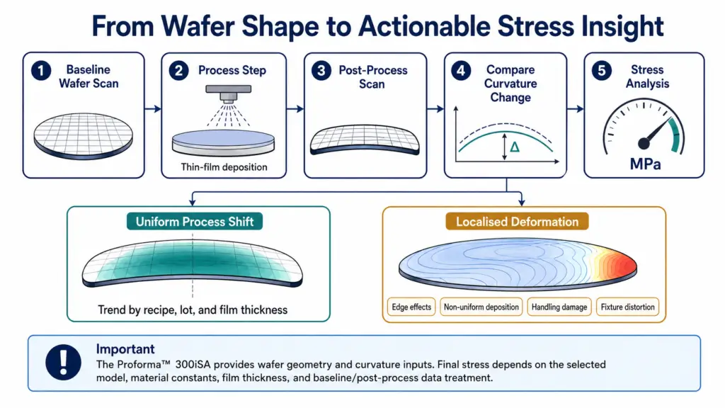
A wafer has a measurable shape before processing. After deposition, etch, thermal treatment, chemical-mechanical planarization (CMP), bonding, or another process step, that shape may change. The curvature difference between the baseline wafer and the processed wafer provides the key input for a stress calculation.
For a meaningful result, the measurement system must provide:
- High repeatability across the wafer surface
- Sufficient spatial coverage to characterise full-wafer behavior
- Non-contact measurement to avoid risk to delicate surfaces
- Consistent, repeatable scan patterns
- Practical data export for engineering analysis and process records
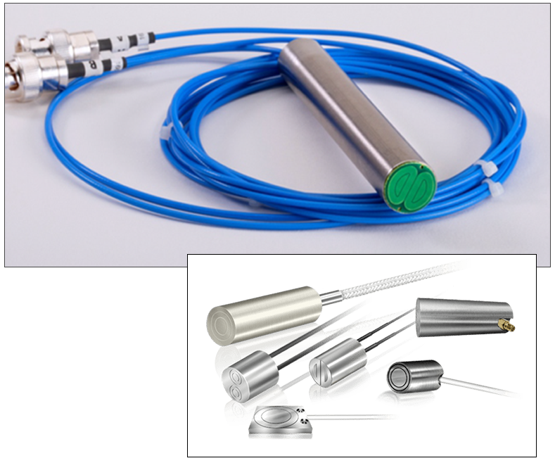
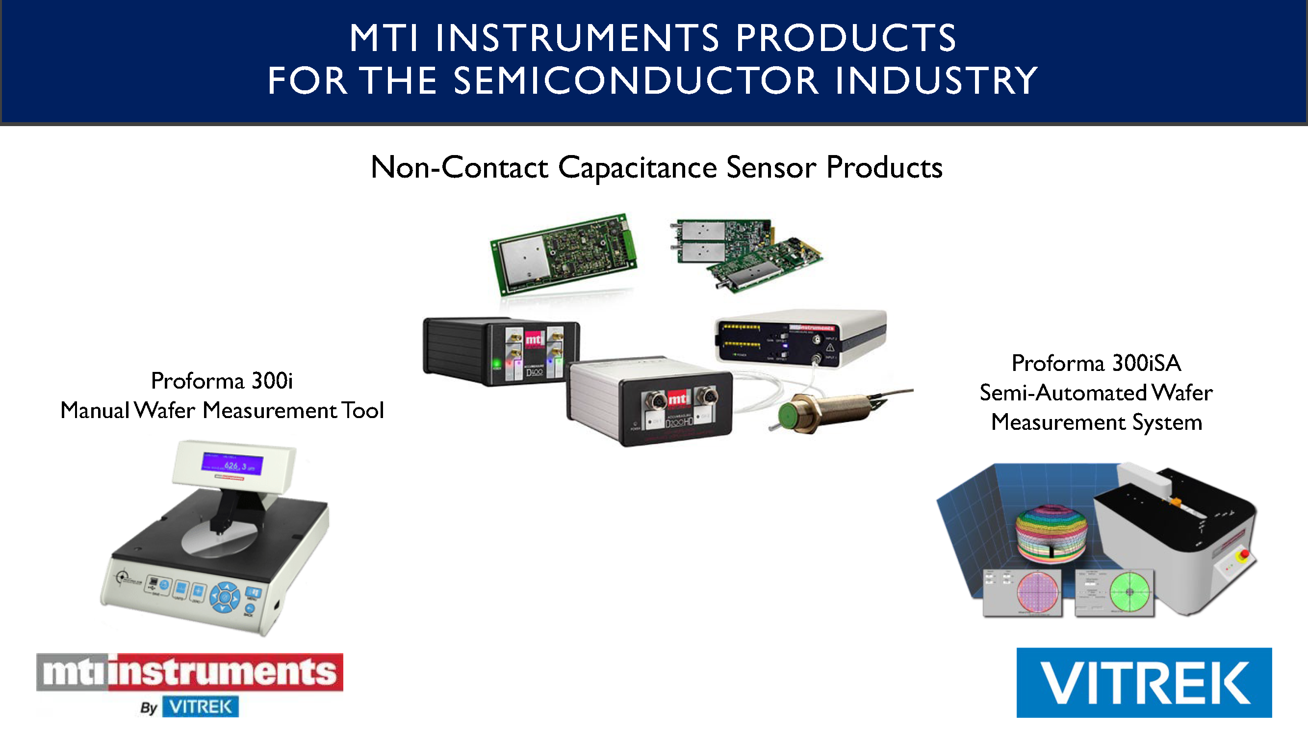
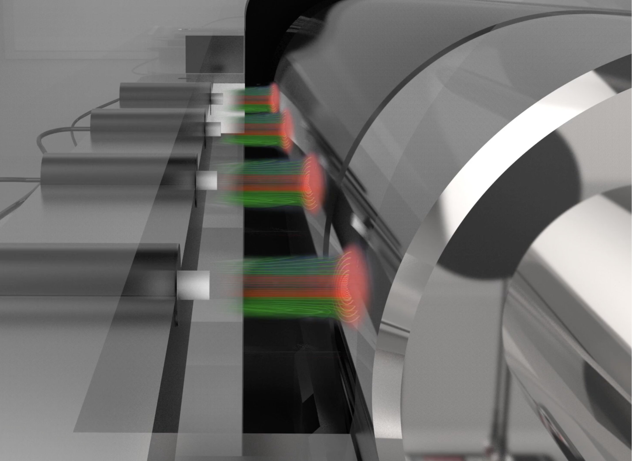
The Proforma™ 300iSA addresses these needs with full-wafer, non-contact capacitance-based measurement. The system performs semi-automated scans of semiconducting and semi-insulating wafers and generates detailed wafer geometry data for thickness, thickness variation, bow, warp, sori, site flatness, and global flatness.
Its full-wafer scanning capability makes it especially useful for stress-characterization workflows, because local measurements alone may not reveal the complete deformation pattern caused by a deposited film or process excursion.
How the Proforma iSA Supports Stress Analysis
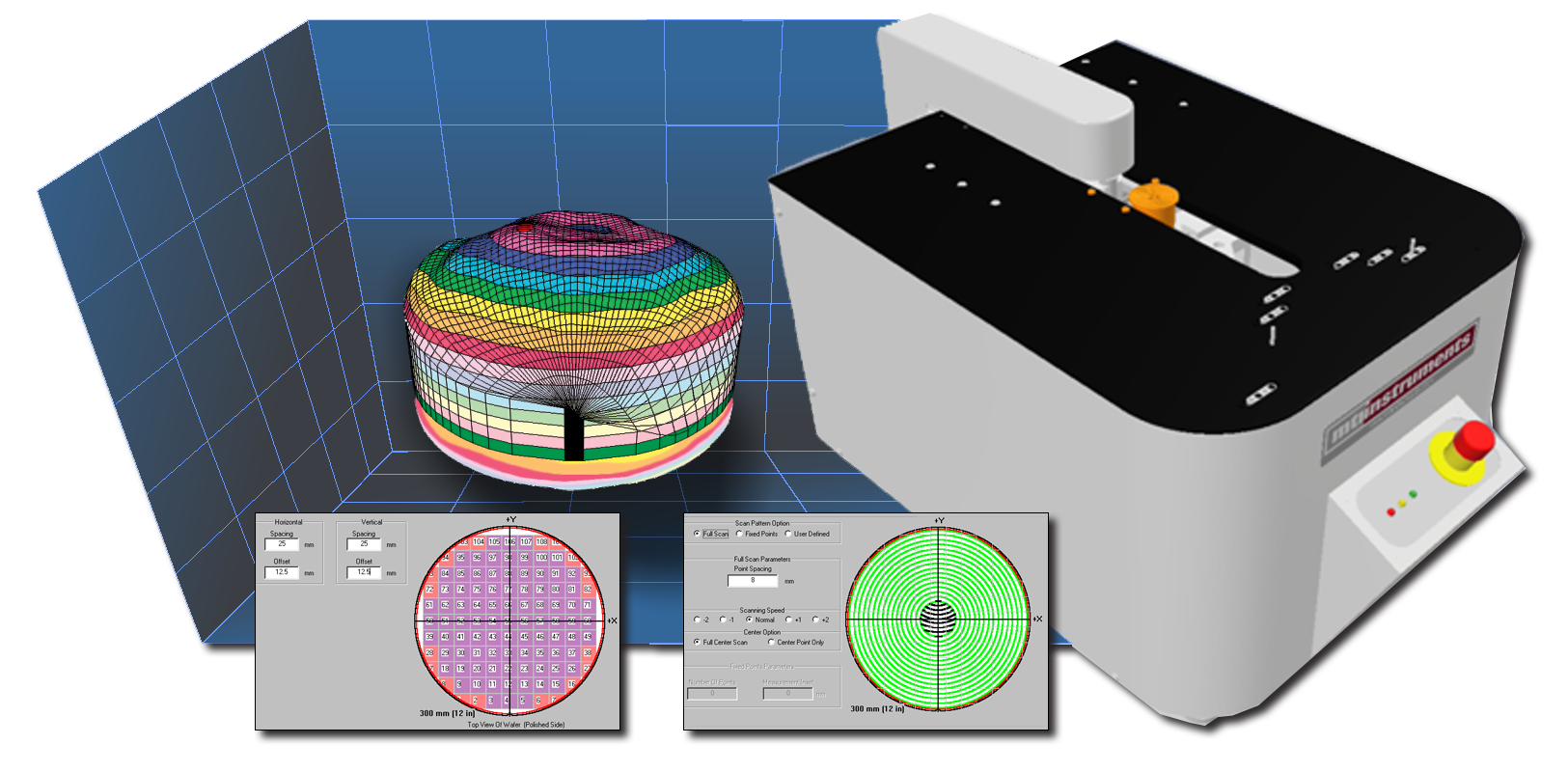
The Proforma™ 300iSA uses MTI’s Push-Pull capacitance technology to make non-contact measurements across the wafer. User-defined and ASTM/SEMI-compliant scan patterns can generate full-wafer three-dimensional images and tabular reports that can be exported for additional analysis.
For stress characterization, the system is used to establish a precise baseline before processing and then measure the wafer again after the relevant process step. Comparing the two datasets enables engineers to determine the change in wafer curvature.
Because the Proforma™ 300iSA captures full-wafer data, teams can review both the overall curvature change and the shape of the deformation. This helps distinguish a uniform process shift from a localized condition such as edge effects, non-uniform deposition, handling damage, or fixture-related distortion.
Film Stress-Characterization Workflow
Consider a process engineer evaluating a new PVD deposition recipe. The objective is to determine whether a revised power setting changes film stress enough to create downstream lithography or wafer-handling risk.
The engineer begins with a representative set of wafers and creates a repeatable Proforma™ 300iSA scan recipe. Each wafer is measured before deposition to establish its individual baseline condition. Following deposition, the same wafers are scanned again.
The pre- and post-process datasets are compared to determine the curvature change for each wafer. The engineer then applies the selected substrate constants, measured film thickness, and stress model to calculate the resulting MPa value. The resulting dataset may reveal several important conditions:
- The new recipe produces lower average stress than the previous recipe
- Stress variation is increasing from wafer to wafer
- Edge behavior differs from centre-of-wafer behavior
- One chamber produces a repeatable curvature signature not seen in others
- A change in film thickness—not deposition chemistry—is responsible for a stress shift
This approach transforms a general observation such as “the wafer is bowing more” into a repeatable, quantitative engineering metric that can be trended and correlated to process conditions.
Key Applications
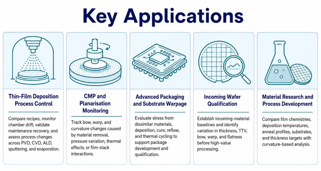
From thin-film deposition and CMP through advanced packaging, incoming qualification, and materials research, full-wafer stress characterization gives semiconductor teams a consistent way to identify and control process-driven geometry change. By measuring curvature, bow, warp, thickness, and flatness
before and after critical steps, engineers can detect variation earlier, compare process conditions with confidence, and protect yield, reliability, and production stability.
Why Use the Proforma 300iSA
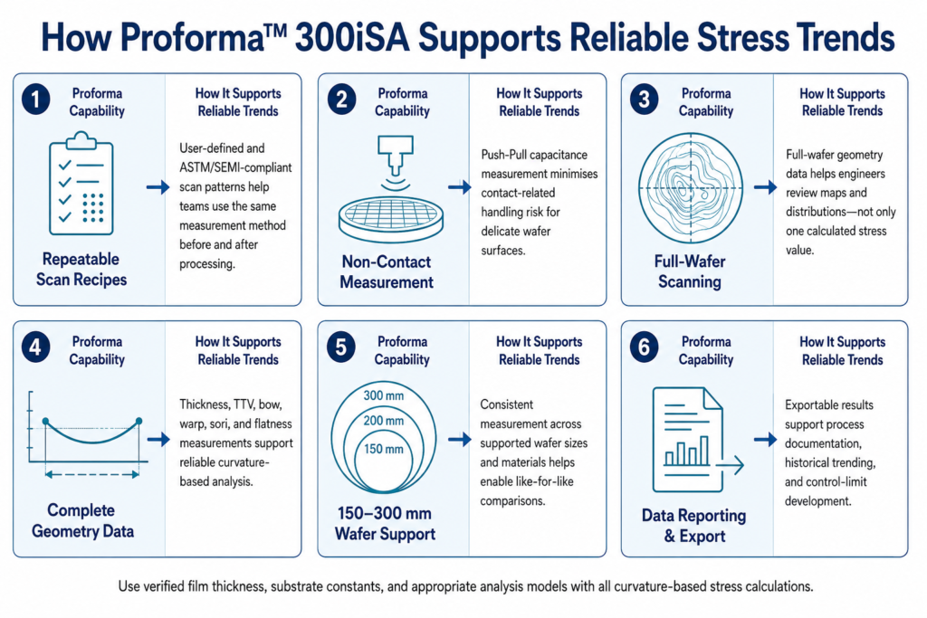
The Proforma™ 300iSA provides a repeatable, non-contact metrology foundation for reliable stress trending. It combines full-wafer geometry measurement with consistent scan methods and exportable data, helping engineers move from individual wafer results to meaningful process insight.
As shown below, each capability supports a more controlled stress-characterization workflow—from protecting high-value wafer surfaces and applying repeatable recipes to reviewing full-wafer patterns, comparing like-for-like material conditions, and documenting results for long-term trend analysis and
control-limit development.
Conclusion
Thin-film stress can influence nearly every stage of semiconductor manufacturing, from deposition and lithography through packaging and reliability. Measuring and trending that stress in MPa gives process teams an earlier, more actionable view of wafer behavior.
The Proforma™ 300iSA provides the data required to support curvature-based stress analysis. By comparing baseline and post-process wafer geometry, engineers can calculate film stress using established models, identify process variation, and make better-informed decisions about recipes, materials, equipment, and quality control.
With full-wafer scanning, repeatable measurement routines, and exportable data, the Proforma™ 300iSA helps transform wafer curvature from a downstream problem into a controlled process variable.