A deposited film can be electrically functional and still fail its process window because it is 8 nm too thin at the wafer edge. That is why semiconductor thickness measurement principles are not simply about obtaining a number. They are about establishing a traceable relationship between an instrument signal, the material stack, the measurement location, and the actual physical thickness required by the device process.
For process engineers and metrology teams, the practical question is rarely which technique has the finest published resolution. The better question is which method produces repeatable, accurate, and actionable thickness data for a specific film, substrate, pattern condition, and production environment.
Why Thickness Is a Process-Critical Parameter
Thickness affects far more than dimensional compliance. In dielectric films, it influences capacitance, breakdown behavior, leakage current, and isolation performance. In metal layers, it affects sheet resistance, current-carrying capability, and subsequent patterning. Epitaxial, photoresist, and compound semiconductor layers each introduce their own relationships between thickness, material properties, and downstream yield.
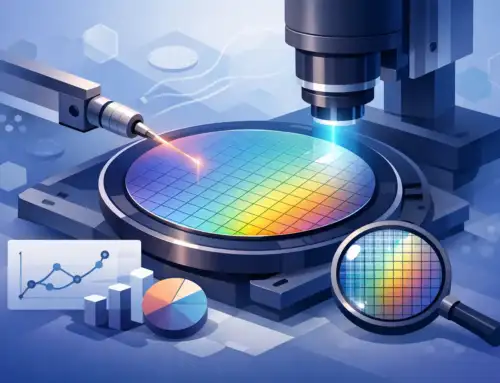
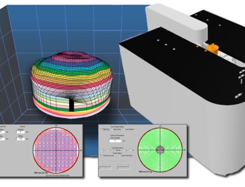
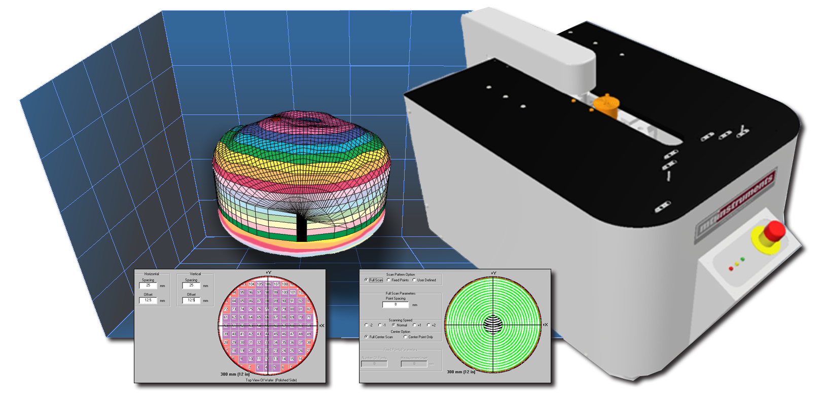
A wafer may also be within specification at its center while showing unacceptable radial variation. Thickness metrology therefore commonly addresses several related outputs: mean thickness, within-wafer nonuniformity, edge exclusion behavior, site-to-site repeatability, and wafer-to-wafer process drift. A single-point reading cannot establish all of these characteristics.
The measurement system must also distinguish between true process variation and apparent variation introduced by surface roughness, film refractive-index changes, wafer bow, vibration, alignment error, or model assumptions. That distinction determines whether an engineer adjusts a deposition recipe, investigates tool hardware, or questions the measurement itself.
Semiconductor Thickness Measurement Principles by Method
No universal technique is appropriate for every semiconductor layer. Material transparency, thickness range, surface condition, substrate type, pattern density, and whether the measurement is destructive all shape method selection.
Optical interference and reflectometry
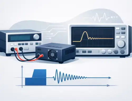
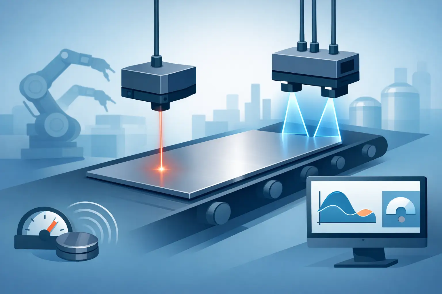
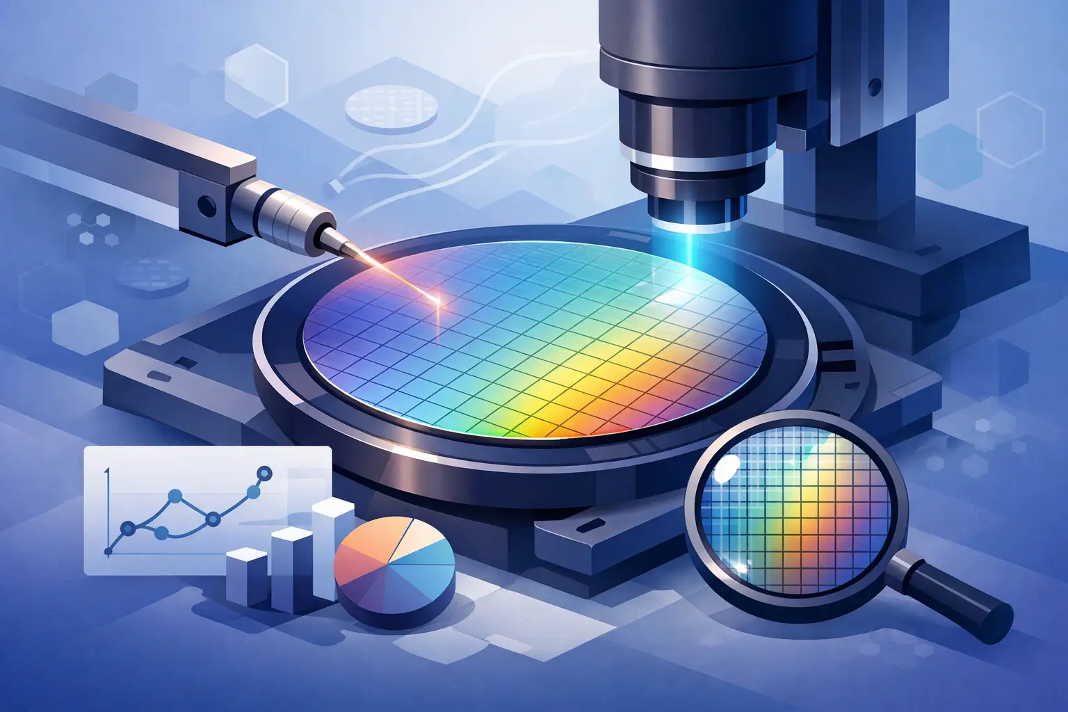
Optical methods use the interaction of light with thin-film interfaces. When light reflects from the top and bottom boundaries of a film, the reflected components can reinforce or cancel one another at different wavelengths. The resulting spectral pattern contains information about optical thickness, which is the product of physical thickness and refractive index.
Spectroscopic reflectometry measures reflected intensity across a range of wavelengths and fits the data to a model of the film stack. It is widely used because it is fast, noncontact, and suitable for thin transparent or semitransparent films. Its performance depends on a valid dispersion model for refractive index and extinction coefficient, accurate knowledge of the underlying layers, controlled spot placement, and a surface that does not scatter excessive light.
The central trade-off is model dependence. If a deposited film’s optical constants shift with density, composition, temperature history, or porosity, a thickness result based on nominal optical properties can be biased. For critical layers, engineers should validate the model against reference samples or an independent measurement method rather than treating the refractive-index library as fixed truth.
Interferometry
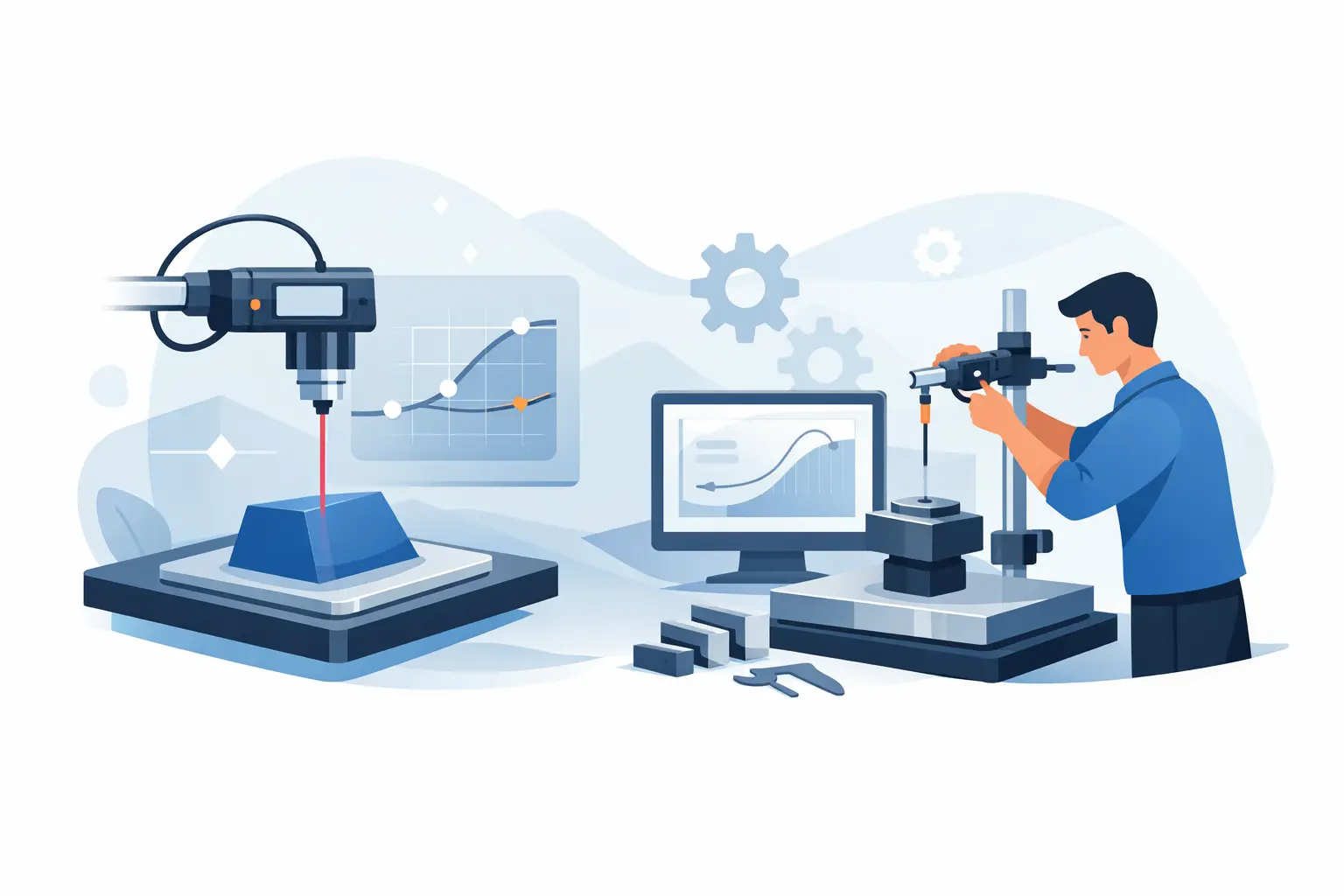
Interferometric techniques compare light reflected from a test surface with light from a reference path or reference surface. Changes in optical path length produce interference fringes that can be analyzed for height, step, or thickness information. White-light interferometry is especially useful for measuring film thickness through a defined step, such as a patterned region adjacent to an etched-open reference area.
This approach directly measures a physical height difference rather than inferring thickness from optical constants. It can provide excellent vertical sensitivity, but it requires an accessible step or suitable geometry. Highly sloped features, very rough surfaces, transparent multilayer structures, and vibration can complicate interpretation. The instrument’s lateral resolution and numerical aperture also matter when the measurement site is small or patterned.
Noncontact displacement measurement
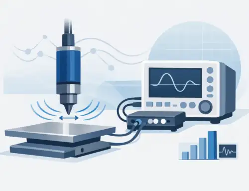
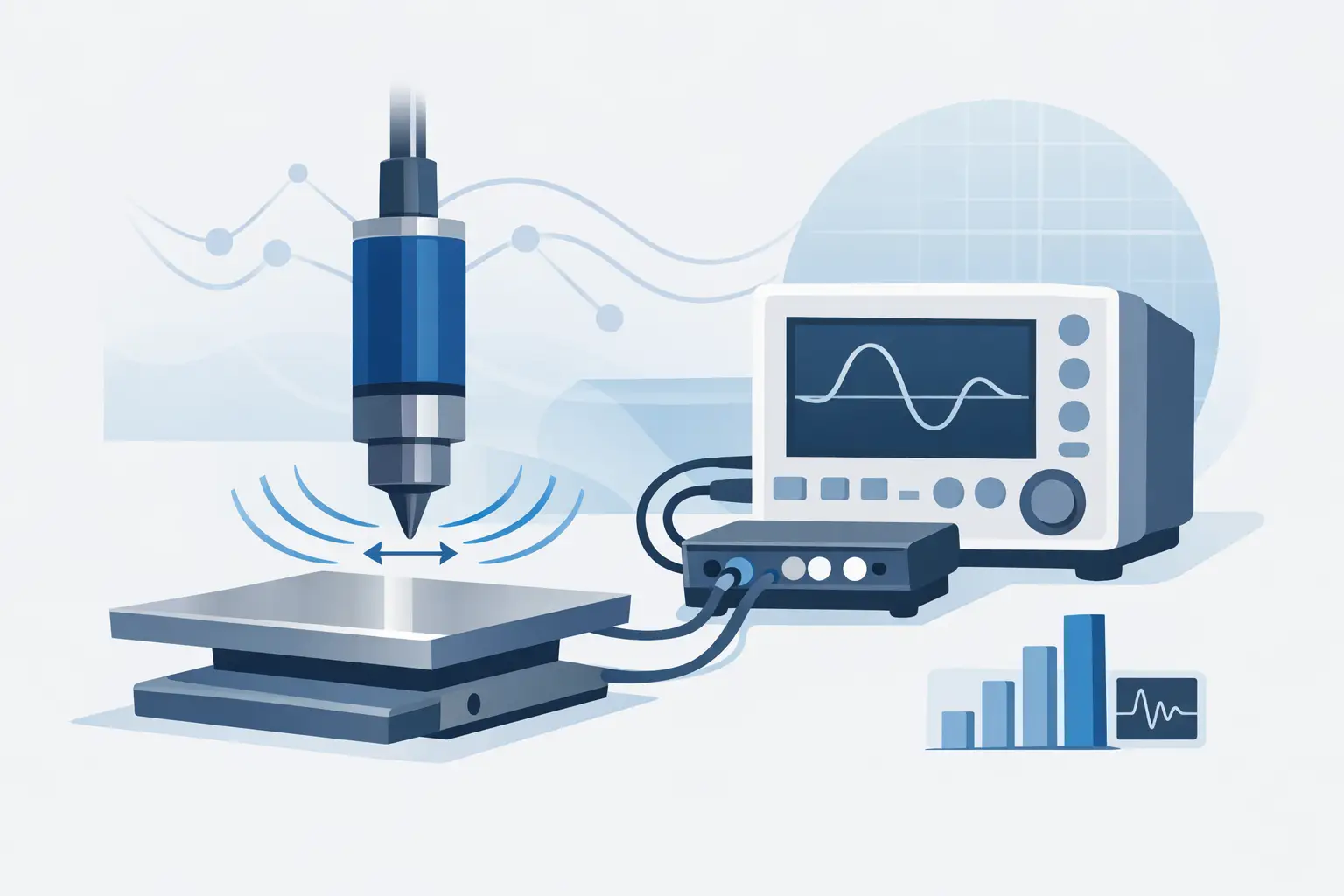
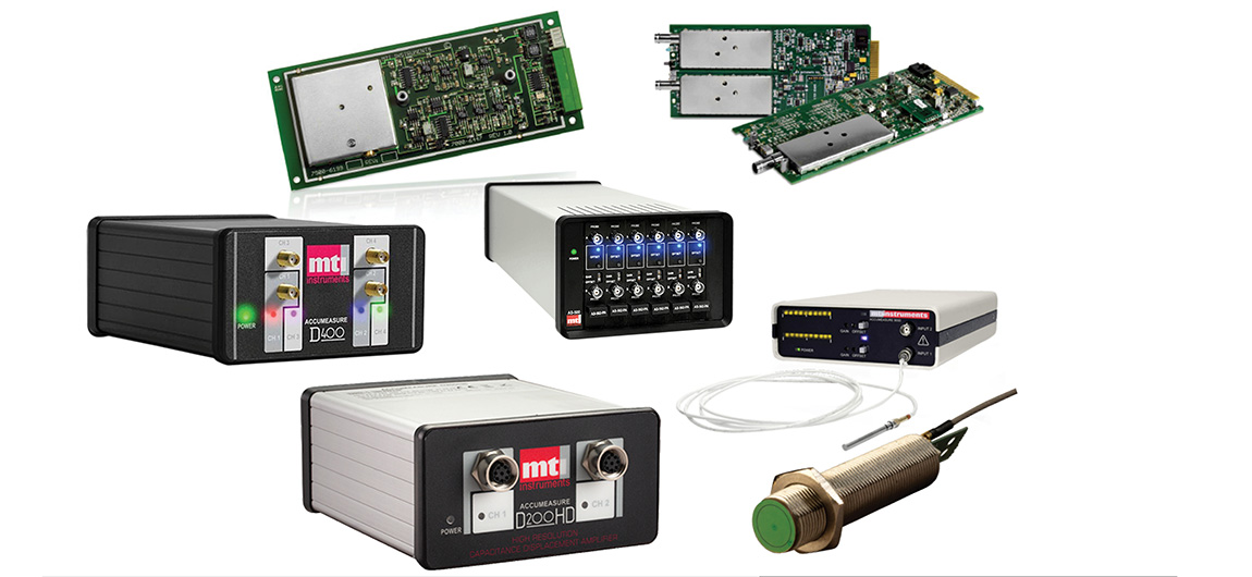
Capacitive, confocal chromatic, and other noncontact displacement sensors measure the position of one or both wafer surfaces. With appropriate fixturing and calibration, thickness can be calculated as the separation between those surfaces. This is particularly useful for substrates, wafers, and films where total thickness variation is the primary concern.
For double-sided thickness measurement, synchronization is essential. Any timing mismatch, wafer motion, stage runout, or variation in the sensor-to-surface response becomes part of the error budget. Capacitive sensing can offer high resolution on conductive targets but depends on material electrical properties and target geometry. Optical displacement methods can accommodate a wider material range, although surface reflectivity and transparency require careful sensor selection.
Mechanical and destructive reference methods
Contact profilometry measures a surface step using a stylus. Cross-sectional scanning electron microscopy can reveal individual layer dimensions at high magnification. These methods may be slower, localized, or destructive, but they remain valuable as reference techniques when qualifying a noncontact process monitor or resolving disagreement between measurements.
Their limitations are practical as well as technical. Stylus force can affect soft films, and cross-section preparation can introduce artifacts. Neither approach alone represents full-wafer uniformity. Used strategically, however, they provide an independent check on model-based optical results.
Measurement Models Matter as Much as Hardware
A thickness instrument does not measure in isolation. It measures a signal and converts that signal through physics, calibration data, and software assumptions. In optical metrology, the assumed layer stack may include film thickness, refractive index, extinction coefficient, surface roughness, interface layers, and substrate optical properties. In displacement systems, the model includes sensor calibration, reference plane definition, fixturing geometry, and stage position.
Model complexity should match the process. An oversimplified model can force a poor fit and report a plausible but incorrect thickness. An overly complex model can create parameter correlation, where multiple combinations of thickness and optical constants fit the same data. The goal is not the maximum number of adjustable parameters. It is a physically defensible model with stable results across representative wafers.
Patterned wafers introduce another constraint. A measurement spot that spans metal, dielectric, and open areas may not represent any single film condition. Site definitions should account for pattern density, local topography, scribe-line availability, and the lateral size of the optical or sensor spot. Measurements taken on monitor wafers must also be shown to correlate with product wafers before they are used for process control.
Building a Defensible Uncertainty Budget
Resolution is not accuracy, and repeatability is not traceability. A system can repeatedly report a value to sub-nanometer increments while carrying a larger systematic error from calibration, material modeling, or setup geometry.
A defensible uncertainty budget considers instrument repeatability, calibration standard uncertainty, environmental effects, sample positioning, surface condition, operator influence, and the measurement model. For an optical method, refractive-index uncertainty and layer-stack assumptions may dominate. For a dual-sided displacement system, fixture stability, sensor alignment, and wafer motion may be the primary contributors.
Environmental control is often underestimated. Temperature affects stage dimensions, sensor electronics, and material properties. Vibration can corrupt high-resolution noncontact measurements. Particles and backside contamination can alter wafer seating, creating apparent thickness changes that are actually handling artifacts. In a production setting, measurement system analysis should include repeated loading and unloading, multiple operators where applicable, and samples spanning the intended thickness range.
Calibration traceability provides the reference chain, but calibration alone does not validate an application. A calibrated sensor can still produce an unsuitable result if the selected range, target material, measurement angle, sampling rate, or data filtering is wrong for the process. Application-specific correlation and periodic verification are necessary controls.
Selecting the Method for the Decision at Hand
Start with the measurement decision, not the instrument category. If the objective is rapid control of a transparent dielectric deposition, spectroscopic reflectometry may be appropriate. If the requirement is total substrate thickness or total thickness variation, noncontact displacement methods may be a stronger fit. If a patterned step is available and direct height measurement is needed, interferometry can provide a useful independent result.
Consider the required thickness range, allowable uncertainty, lateral sampling area, wafer size, surface finish, throughput, automation interface, and data-management requirements. Semiconductor manufacturing also requires attention to wafer handling, cleanroom compatibility, recipe control, preventive maintenance, calibration intervals, and the ability to retain measurement records for engineering review.
For high-consequence process decisions, use an orthogonal measurement path during development or qualification. Comparing a model-based optical result with a step-height, cross-sectional, or displacement-based measurement can expose assumptions that would otherwise remain hidden. Once correlation is established, the faster production method can be used with substantially greater confidence.
Thickness data earns its value when it closes the loop between deposition, etch, lithography, electrical performance, and yield. The right metrology approach is the one that makes that connection clear enough for an engineer to act before a marginal layer becomes a costly wafer excursion.