_Page_1-header")

Application Overview
Wafer lapping is a critical semiconductor thinning process that demands tight control to avoid over-removal of material, which can lead to costly yield loss. This application note details how MTI Instruments’ Accumeasure™ capacitive sensing technology enabled precise, real-time displacement and thickness measurement during lapping operations, ensuring consistent wafer quality.
Challenge
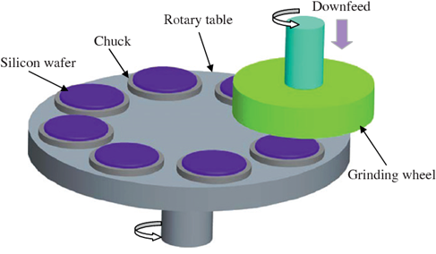
During lapping, wafers are thinned from the backside using a rotating abrasive surface. As the process proceeds, precise feedback is essential to monitor how much material is removed and to determine the wafer’s final thickness. Traditional mechanical methods or visual inspections are not sensitive or fast enough for today’s semiconductor manufacturing tolerances.
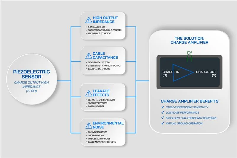
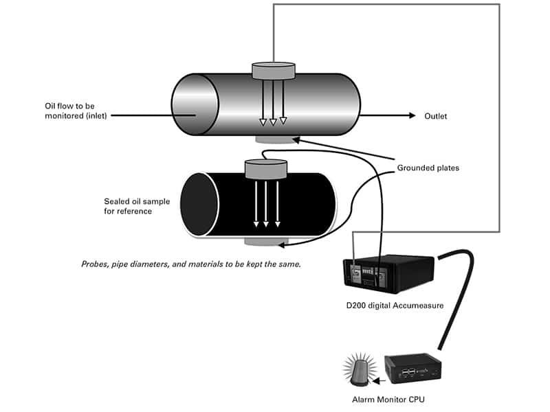
The Solution: MTI’s Non-Contact Capacitance-Based Measurement System
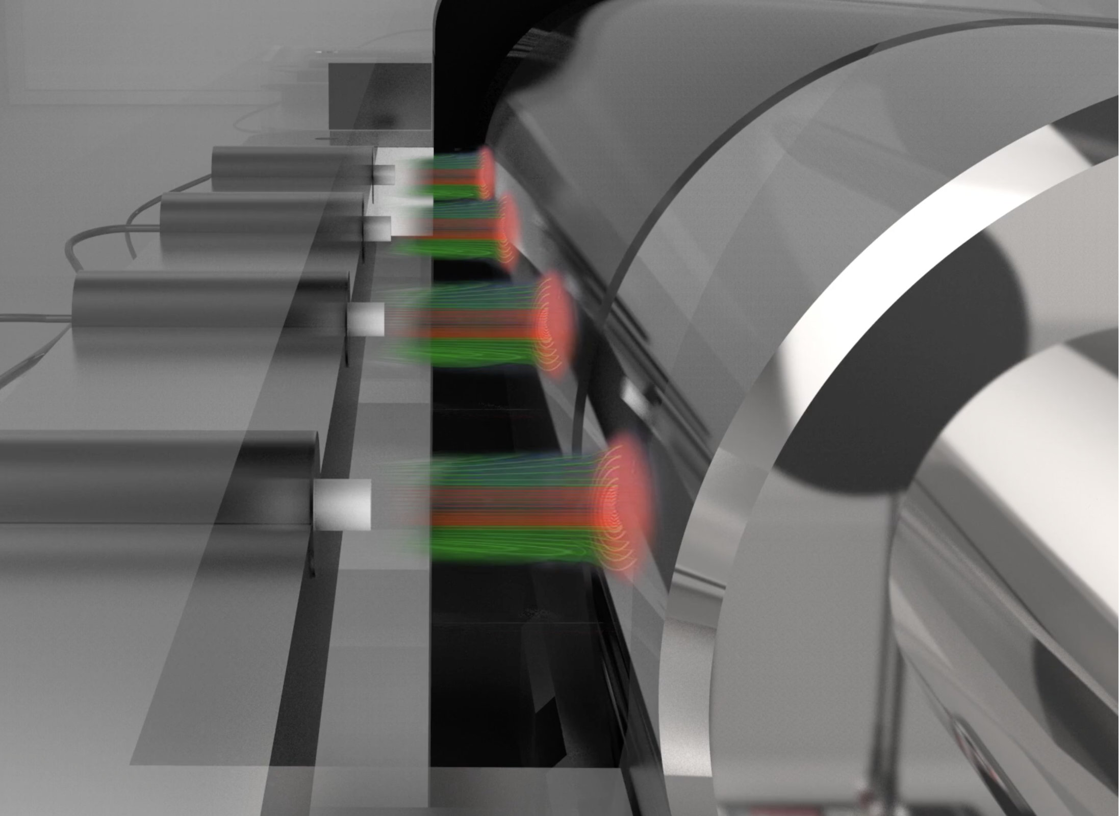
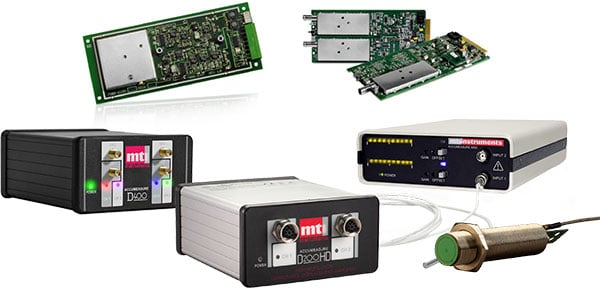
 MTI’s Accumeasure™ high resolution system using push-pull capacitance probes to monitor displacement with sub-micron accuracy, even in an electrically noisy, rotating lapping environment.
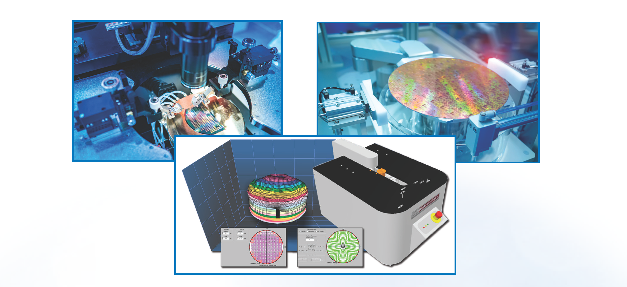
Lapping System Overview
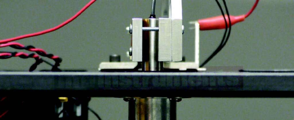
• A semiconductor wafer was sandwiched between a Pyrex plate and a fluid barrier above the rotating lapping wheel.
• A metal weight applied constant downward pressure, simulating production conditions.
• MTI’s push-pull capacitance probe was mounted above the floating weight (which was electrically ungrounded).
• A second probe tracked vertical displacement of the lapping plate.
As the wafer thinned, the metal weight gradually dropped. The relative displacement between the weight and the lapping plate directly corresponded to material removed from the wafer.
— Real-time, non-contact measurement ensures precise wafer thinning and prevents over-lapping —
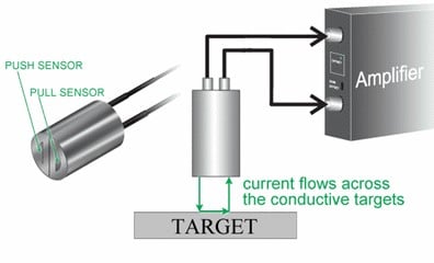
Why Push-Pull Probes?
MTI’s push-pull probes deliver highly accurate displacement measurements—even when the target is ungrounded or rotating. Unlike single-ended probes, pushpull
designs use dual, out-of-phase signals that flow across the target surface, eliminating grounding errors and noise interference. This makes them perfectly suited for dynamic environments where consistent, high-resolution data is essential for process control.
Data Acquisition & Signal Processing
Data from both probes are digitized using MTI’s amplifier and analyzed via LabVIEW software. Key steps included:
- Anti-alias filtering (5 kHz cutoff) and 20 kSPS sampling rate.
- Median signal extraction to reject groove-induced spikes on the lapping plate.
- Auto-zeroing at process start to establish a thickness baseline
- Real-time monitoring of the gap change between the weight and the plate.
Groove noise and surface irregularities are smoothed via custom LabVIEW routines using boxcar averaging and sample-based median filtering.
Results: Accurate, Real-Time Wafer Thickness Calculation
Using MTI’s Accumeasure system, customers achieve accurate, real-time monitoring of wafer thickness throughout the lapping process. By continuously measuring the displacement between the lapping weight and the plate, the system precisely calculates the amount of material removed. The initial wafer thickness was compared to the measured loss to determine the current thickness at any given moment.
Automated alarms signaled when the desired thinning was reached, allowing the process to stop before over-lapping occurred. This approach significantly improved process consistency, reduced scrap, and enhanced overall yield.
Conclusion
MTI’s Accumeasure system enabled this semiconductor customer to maintain tight control over wafer thinning with unmatched precision and automated process feedback. The result was improved yield, throughput, and quality control in a key fabrication step.
System Benefits
- Non-contact, high-precision thickness tracking
- Real-time feedback for process control
- Reliable in electrically isolated or noisy environments
- Automated alerts to prevent over-lapping
.


