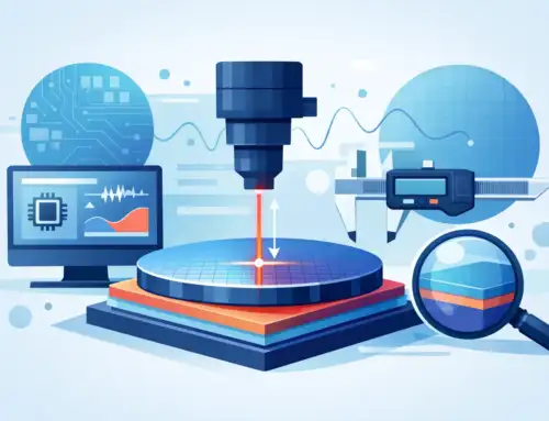
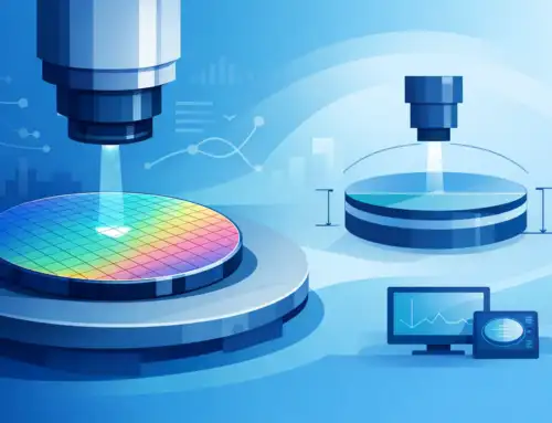
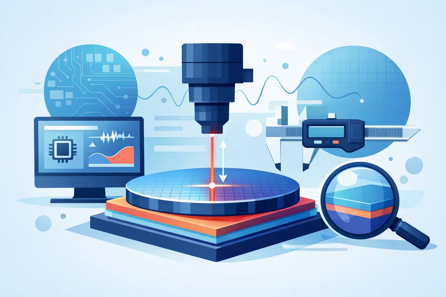
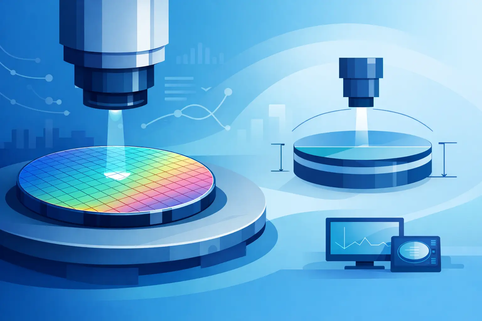
A wafer inspection platform can appear highly capable in a demonstration and still be the wrong instrument for a production line. The best wafer inspection tools are not defined by maximum resolution alone. They are defined by whether they detect the defects that matter, at a sampling rate and throughput that support a usable process-control decision.
For semiconductor engineering teams, the selection process starts with the failure mechanism, not the instrument brochure. A tool intended to monitor incoming bare wafers has a different optical, handling, and data requirement than a system used to identify pattern defects after lithography, inspect backside contamination, or characterize wafer geometry before bonding. Clear requirements protect capital budgets and reduce the risk of collecting large volumes of data that do not improve yield.
What the Best Wafer Inspection Tools Must Deliver
Inspection is often discussed as if it were a single measurement task. In practice, it includes several distinct functions: locating surface defects, identifying particles and contamination, detecting pattern anomalies, examining edge and backside conditions, and providing dimensional or geometric information that affects downstream processing.
The right system must deliver meaningful sensitivity without creating an unmanageable nuisance-defect burden. A tool that flags every benign process variation can consume review capacity and obscure the defects associated with yield loss. Conversely, a high-throughput system that misses the defect population of interest may provide false confidence.
Engineers should define acceptance criteria in measurable terms. These commonly include minimum detectable defect size, defect capture rate, false-alarm rate, wafer coverage, image quality, repeatability, and cycle time. Each metric should be tied to a specific decision: release a wafer lot, adjust a process module, trigger maintenance, quarantine material, or conduct failure analysis.
Sensitivity and throughput are an engineering trade-off
Higher sensitivity often requires more image acquisition, tighter focus control, slower stage motion, or additional optical channels. Those requirements can reduce wafers per hour. This is not inherently a problem in an R&D lab or low-volume failure-analysis workflow, where information quality is the priority. It becomes a significant constraint in high-volume manufacturing, where delayed feedback can allow a process excursion to affect many wafers.
The useful question is not, “What is the smallest defect this tool can see?” It is, “What defect size and type must be detected at the required confidence level on this layer, at this production rate?” That distinction prevents teams from paying for sensitivity that does not change an operational decision.
Defect detection is not defect classification
Many inspection systems can identify a signal that differs from the expected wafer surface or pattern. Fewer systems can reliably classify that signal as a particle, scratch, pit, residue, pattern bridge, missing feature, edge chip, or another defect class without review.
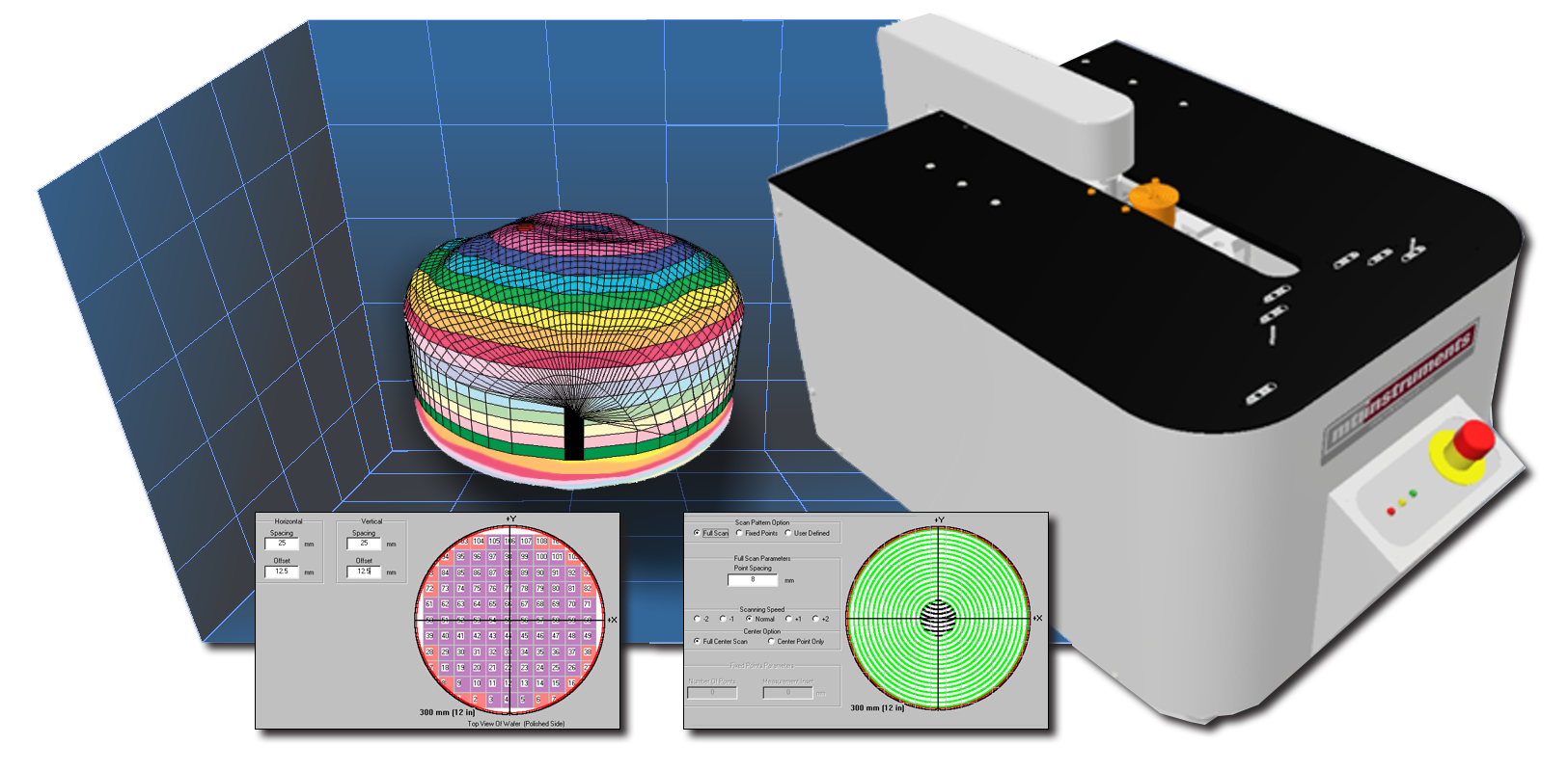
Classification quality matters because corrective action depends on defect source. Random particles may point to contamination control or handling. Repeating pattern defects may indicate an exposure, mask, deposition, etch, or CMP issue. Spatial signatures such as center-to-edge variation, radial rings, or recurring die locations can be as valuable as the individual defect image.
Evaluate how the tool records location, size, intensity, morphology, and classification confidence. The data structure should support wafer maps, lot-to-lot comparisons, excursion analysis, and traceability to the process step. A high-quality image without usable contextual data has limited value in a controlled manufacturing environment.
Match the Inspection Method to the Wafer and Process Step
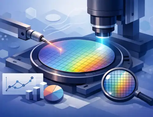
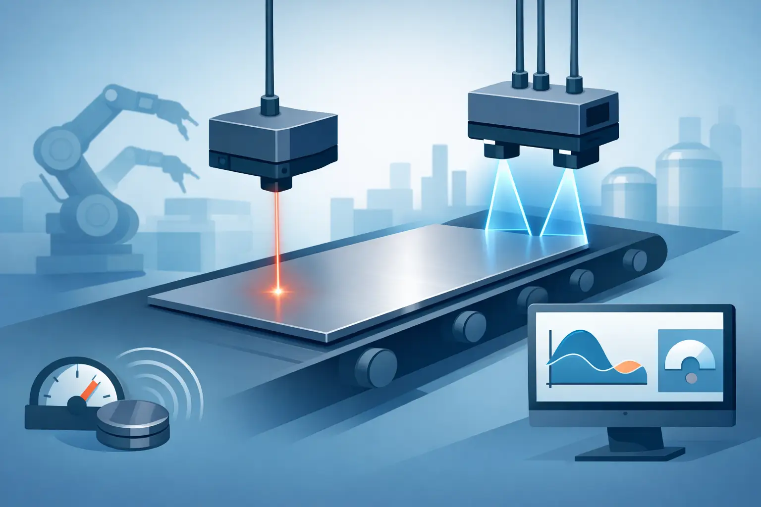
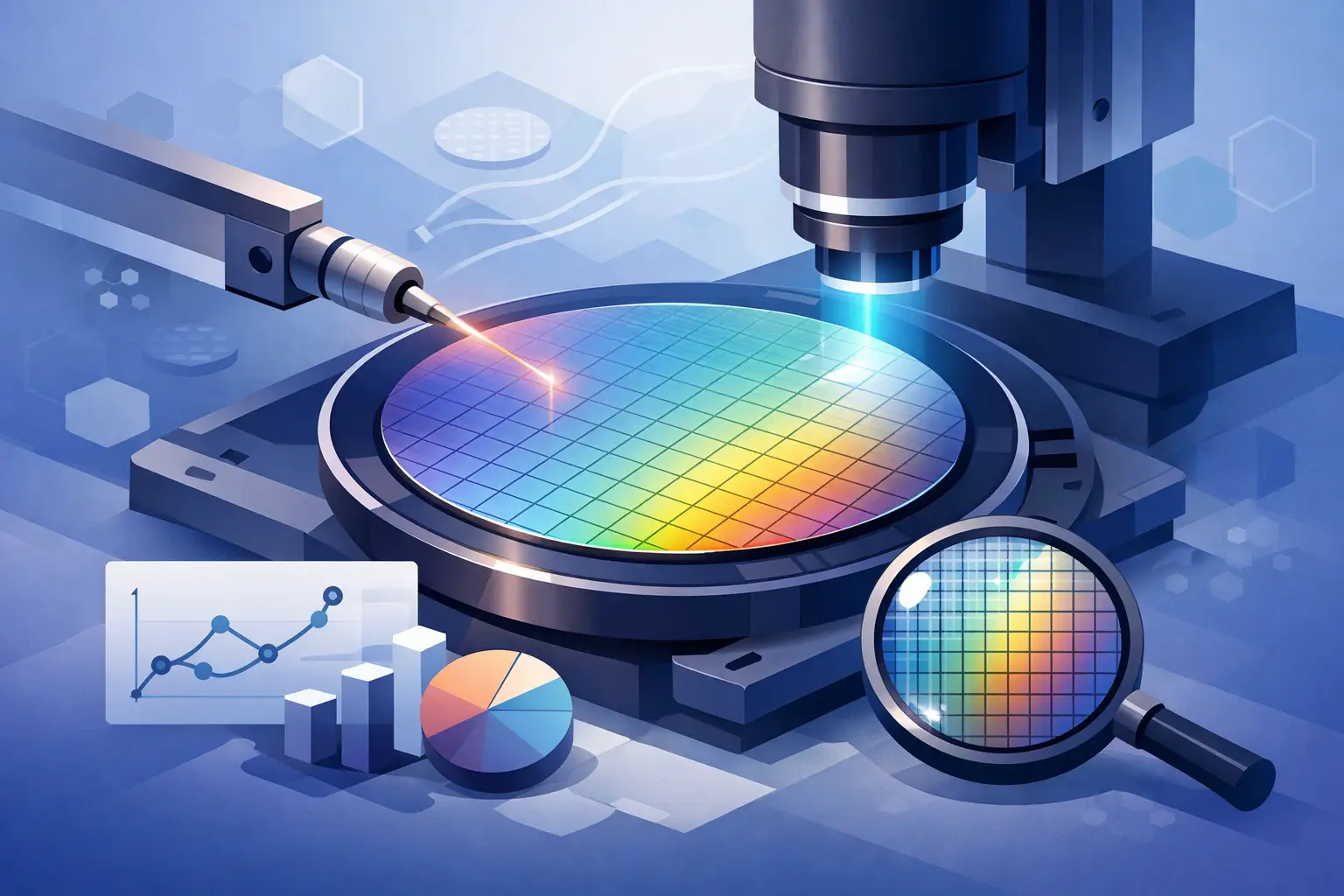
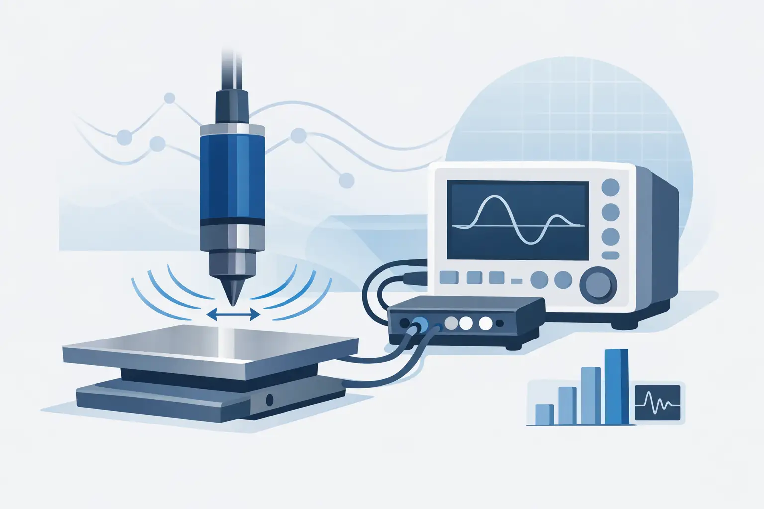
Optical inspection remains a practical choice for many wafer applications because it supports non-contact measurement and can provide useful speed across large areas. Brightfield methods are effective for many surface and pattern inspection tasks. Darkfield methods can improve contrast for scattering defects such as particles, scratches, and certain surface irregularities. The appropriate illumination geometry depends on the defect mechanism, surface finish, film stack, and pattern complexity.
For transparent, multilayer, highly reflective, or otherwise challenging materials, a standard visible-light configuration may not provide enough contrast or depth discrimination. Applications may require multiple wavelengths, polarization control, infrared imaging, confocal techniques, or other specialized approaches. The objective is not to select the most complex optical architecture. It is to establish sufficient contrast between a critical defect and its background under production conditions.
Bare wafers require different capabilities than patterned wafers
Bare-wafer inspection commonly focuses on particles, haze, scratches, pits, slip, edge damage, backside contamination, and surface quality. These tasks may require broad area coverage and strong repeatability for incoming material qualification or process monitoring.
Patterned-wafer inspection introduces die-to-die and cell-to-cell comparison, design-rule context, pattern noise, and layer-specific sensitivity requirements. A signal that is obvious on a polished bare wafer can be difficult to separate from a dense patterned background. Patterned-wafer workflows also place greater emphasis on coordinate accuracy and review integration because defect locations must be correlated with die, reticle field, and process history.
Do not assume that a platform optimized for unpatterned wafer surface defects will provide the required performance on advanced patterned layers. Similarly, a high-complexity patterned-wafer system can be inefficient for routine incoming bare-wafer screening.
Consider edge, backside, and geometry as separate requirements
Yield-affecting defects are not limited to the front side. Edge chips, microcracks, bevel contamination, and backside particles can affect handling, lithography focus, bonding, chucking, and device reliability. These conditions may require dedicated viewing angles, wafer rotation, or handling configurations that are not part of a standard front-side scan.
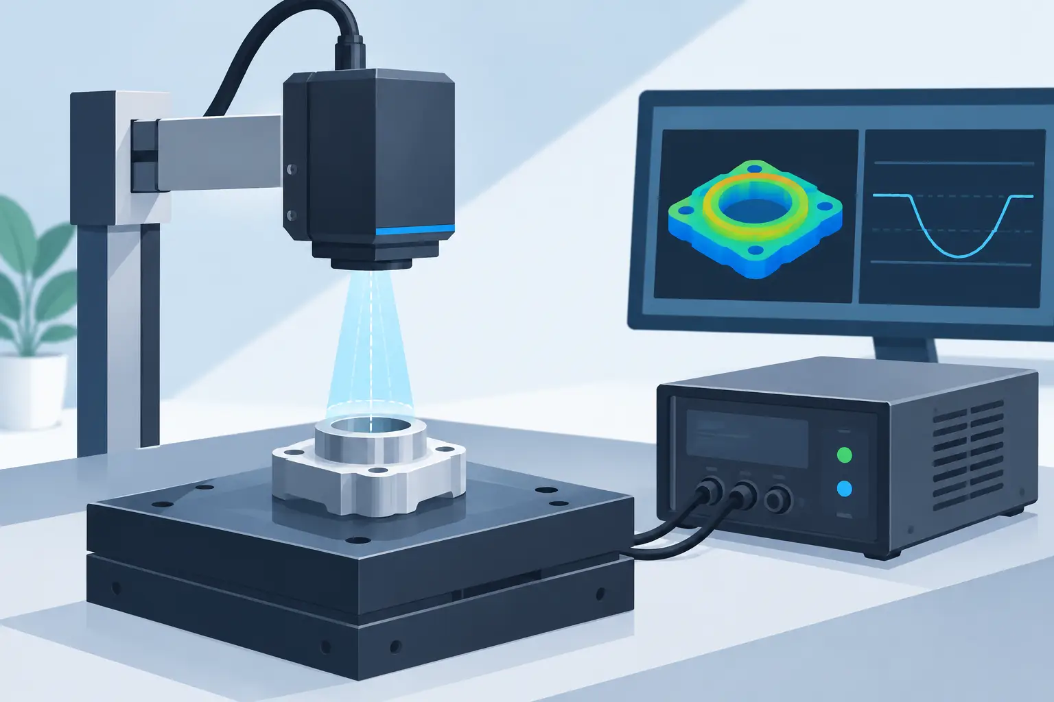
Geometric measurements such as bow, warp, thickness variation, flatness, and surface topography also belong in the broader wafer quality strategy. They are metrology tasks rather than defect inspection tasks, although the process-control decisions often overlap. When a process requires both, evaluate whether the systems can share wafer identification, recipes, maps, and manufacturing data. Integrating results is often more valuable than forcing one instrument to perform every measurement.
Evaluate the Measurement System, Not Only the Sensor
A technically sound inspection tool includes more than optics and image processing. Wafer handling, stage accuracy, focus control, recipe management, calibration approach, software architecture, and serviceability all influence measurement integrity.
For critical applications, verify repeatability using representative wafers and known defect standards where available. Testing should include realistic surface conditions, process films, wafer sizes, and defect distributions. Vendor demonstrations using ideal samples are useful, but they do not replace an application-specific evaluation.
Ask how the tool maintains positional accuracy across the wafer, how it manages focus on warped substrates, and how often calibration or verification is required. Understand whether performance specifications apply at the wafer center only or across the full usable scan area. Also establish the environmental requirements for vibration, temperature stability, cleanliness, and operator interaction. A measurement system that performs well in a controlled laboratory may need additional controls before deployment near production equipment.
Data Integration Determines Process Value
Inspection data must move from image capture to action. The most effective systems support consistent wafer and lot identification, recipe version control, defect maps, exportable results, and traceable audit records. For automated environments, consider the availability of software interfaces, data formats, factory automation compatibility, and the ability to connect results to manufacturing execution systems or statistical process-control workflows.
Data integrity deserves the same attention as optical sensitivity. If operators can change recipes without controls, if defect thresholds are not recorded, or if lot data cannot be traced to a calibration state, the resulting information may be difficult to defend during quality investigations or customer audits.
A practical evaluation should also account for review workflow. Determine who will review flagged defects, how images will be prioritized, and what criteria will trigger engineering action. Inspection capacity is not simply wafers per hour. It is the combined capacity of scanning, review, classification, disposition, and feedback to the process owner.
Build a Selection Specification Before Requesting Quotes
A concise specification gives suppliers a fair basis for proposing a system and gives internal stakeholders a way to compare alternatives. Include the wafer materials, diameters, thickness range, front-side and backside conditions, target defect types, required detection threshold, coverage area, throughput, automation level, data outputs, facility constraints, and calibration expectations.
It is also useful to separate mandatory requirements from desirable capabilities. A facility may need 100 percent backside coverage and lot traceability, while automated classification of every nuisance particle may be desirable but not essential. This distinction helps prevent scope growth and keeps the evaluation focused on yield and compliance risk.
For organizations that require inspection alongside precision geometric measurement, electrical test, or broader manufacturing diagnostics, the supplier’s application knowledge and support model should be evaluated as carefully as the instrument specification. Long-term performance depends on training, method development, calibration traceability, spare-part availability, and the ability to adapt recipes as processes change.
The strongest wafer inspection decision is usually the one that makes the next engineering action clearer. Specify the defects that matter, validate detection on representative wafers, and select a measurement architecture that can sustain the required feedback loop as production and device complexity evolve.